- 您現(xiàn)在的位置:買賣IC網(wǎng) > PDF目錄98012 > MC68HC08KH12FU (MOTOROLA INC) 8-BIT, MROM, 6 MHz, MICROCONTROLLER, PQFP64 PDF資料下載
參數(shù)資料
| 型號: | MC68HC08KH12FU |
| 廠商: | MOTOROLA INC |
| 元件分類: | 微控制器/微處理器 |
| 英文描述: | 8-BIT, MROM, 6 MHz, MICROCONTROLLER, PQFP64 |
| 封裝: | PLASTIC, QFP-64 |
| 文件頁數(shù): | 169/275頁 |
| 文件大小: | 2592K |
| 代理商: | MC68HC08KH12FU |
第1頁第2頁第3頁第4頁第5頁第6頁第7頁第8頁第9頁第10頁第11頁第12頁第13頁第14頁第15頁第16頁第17頁第18頁第19頁第20頁第21頁第22頁第23頁第24頁第25頁第26頁第27頁第28頁第29頁第30頁第31頁第32頁第33頁第34頁第35頁第36頁第37頁第38頁第39頁第40頁第41頁第42頁第43頁第44頁第45頁第46頁第47頁第48頁第49頁第50頁第51頁第52頁第53頁第54頁第55頁第56頁第57頁第58頁第59頁第60頁第61頁第62頁第63頁第64頁第65頁第66頁第67頁第68頁第69頁第70頁第71頁第72頁第73頁第74頁第75頁第76頁第77頁第78頁第79頁第80頁第81頁第82頁第83頁第84頁第85頁第86頁第87頁第88頁第89頁第90頁第91頁第92頁第93頁第94頁第95頁第96頁第97頁第98頁第99頁第100頁第101頁第102頁第103頁第104頁第105頁第106頁第107頁第108頁第109頁第110頁第111頁第112頁第113頁第114頁第115頁第116頁第117頁第118頁第119頁第120頁第121頁第122頁第123頁第124頁第125頁第126頁第127頁第128頁第129頁第130頁第131頁第132頁第133頁第134頁第135頁第136頁第137頁第138頁第139頁第140頁第141頁第142頁第143頁第144頁第145頁第146頁第147頁第148頁第149頁第150頁第151頁第152頁第153頁第154頁第155頁第156頁第157頁第158頁第159頁第160頁第161頁第162頁第163頁第164頁第165頁第166頁第167頁第168頁當前第169頁第170頁第171頁第172頁第173頁第174頁第175頁第176頁第177頁第178頁第179頁第180頁第181頁第182頁第183頁第184頁第185頁第186頁第187頁第188頁第189頁第190頁第191頁第192頁第193頁第194頁第195頁第196頁第197頁第198頁第199頁第200頁第201頁第202頁第203頁第204頁第205頁第206頁第207頁第208頁第209頁第210頁第211頁第212頁第213頁第214頁第215頁第216頁第217頁第218頁第219頁第220頁第221頁第222頁第223頁第224頁第225頁第226頁第227頁第228頁第229頁第230頁第231頁第232頁第233頁第234頁第235頁第236頁第237頁第238頁第239頁第240頁第241頁第242頁第243頁第244頁第245頁第246頁第247頁第248頁第249頁第250頁第251頁第252頁第253頁第254頁第255頁第256頁第257頁第258頁第259頁第260頁第261頁第262頁第263頁第264頁第265頁第266頁第267頁第268頁第269頁第270頁第271頁第272頁第273頁第274頁第275頁
Preliminary Electrical Specications
Advance Information
MC68HC(7)08KH12 — Rev. 1.0
250
Preliminary Electrical Specifications
MOTOROLA
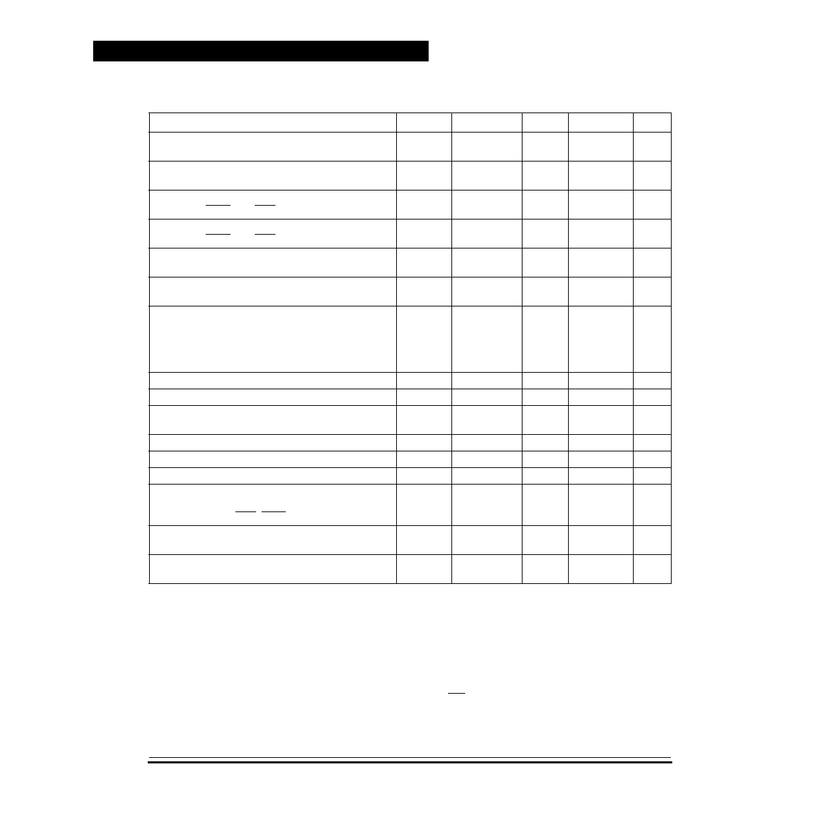
17.6 DC Electrical Characteristics
Characteristic
Symbol
Min
Typ(2)
Max
Unit
Output High Voltage
(ILOAD = –2.0mA) All I/O Pins
VOH
VDD – 0.8
—
V
Output Low Voltage
(ILOAD = 1.6mA) All I/O Pins
VOL
—
0.4
V
Input High Voltage
All ports, IRQ1/V
PP, RST, OSC1
VIH
0.7
× V
DD
—VDD
V
Input Low Voltage
All ports, IRQ1/V
PP, RST, OSC1
VIL
VSS
—
0.3
× V
DD
V
Output High Current
(VOH = 2.1V) Port C in LDD mode
IOH
3
4.5
6
mA
Output Low Current
(VOL = 2.3V) Port C in LDD mode
IOL
10
15
20
mA
VDD Supply Current
Run, USB active, PLL on, fOP = 6.0MHz
(3)
Run, USB suspended, PLL off, fOP = 1.5MHz
(3)
Wait (4)
Stop(5)
0
°C to 85°C
IDD
—
20
3
1
350
mA
A
I/O Ports Hi-Z Leakage Current
IIL
——
±10
A
Input Current
IIN
——
±1
A
Capacitance
Ports (as Input or Output)
COUT
CIN
—
12
8
pF
POR ReArm Voltage(6)
VPOR
0
—
100
mV
POR Rise Time Ramp Rate(7)
RPOR
0.035
—
V/ms
Monitor Mode Entry Voltage
VDD+VHI
1.4
× V
DD
2.0
× V
DD
V
Pullup resistor
PA0-PA7, PB0-PB7, PC0-PC7, PD0-PD7, PE0-
PE3, PF0-PF7, RST, IRQ1/V
PP
RPU
20
35
50
k
Schmitt Trigger Input High Level
PD0-PD7, PE0-PE3, PF0-PF7
VSHI
2.8
3.4
V
Schmitt Trigger Input Low Level
PD0-PD7, PE0-PE3, PF0-PF7
VSHL
1.7
2.3
V
NOTES:
1. VDD = 4.0 to 5.5 Vdc, VSS = 0 Vdc, TA = TL to TH, unless otherwise noted.
2. Typical values reflect average measurements at midpoint of voltage range, 25
°C only.
3. Run (operating) IDD measured using external square wave clock source. All inputs 0.2 V from rail. No dc loads. Less than 100 pF on
all outputs. CL = 20 pF on OSC2. All ports configured as inputs. OSC2 capacitance linearly affects run IDD. Measured with all modules
enabled.
4. Wait IDD measured using external square wave clock source (fCGMXCLK = 6 MHz); all inputs 0.2 V from rail; no dc loads; less than 100
pF on all outputs. CL = 20 pF on OSC2; USB in suspend mode, 15 K ± 5% termination resistors on D+ and D– pins; all ports con-
figured as inputs; OSC2 capacitance linearly affects wait IDD.
5. STOP IDD measured with USB in suspend mode, OSC1 grounded, 1.425 K ± 1% pull-up resistor on D+ pin and 15 K ± 1% pull-
down resistors on D+ and D– pins, no port pins sourcing current.
6. Maximum is highest voltage that POR is guaranteed.
7. If minimum VDD is not reached before the internal POR reset is released, RST must be driven low externally until minimum VDD is
reached.
8. RPU is measured at VDD = 5.0V.
相關(guān)PDF資料 |
PDF描述 |
|---|---|
| MC68HC08XL36CB | 8-BIT, MROM, 8.2 MHz, MICROCONTROLLER, PDIP56 |
| MC68HC11A0FNR2 | 8-BIT, MICROCONTROLLER, PQCC52 |
| MC68HC11A8FN1R2 | 8-BIT, MROM, MICROCONTROLLER, PQCC52 |
| MC68HC11E0CFNE2R2 | 8-BIT, MROM, 3 MHz, MICROCONTROLLER, PQCC52 |
| MC68HC11KG4CPU4 | 8-BIT, MROM, 4.2 MHz, MICROCONTROLLER, PQFP100 |
相關(guān)代理商/技術(shù)參數(shù) |
參數(shù)描述 |
|---|---|
| MC68HC08KL8B | 制造商:FREESCALE 制造商全稱:Freescale Semiconductor, Inc 功能描述:General Release Specification |
| MC68HC08KL8FB | 制造商:FREESCALE 制造商全稱:Freescale Semiconductor, Inc 功能描述:General Release Specification |
| MC68HC08KX8 | 制造商:MOTOROLA 制造商全稱:Motorola, Inc 功能描述:Microcontrollers |
| MC68HC08LJ12 | 制造商:FREESCALE 制造商全稱:Freescale Semiconductor, Inc 功能描述:Addendum to MC68HC908LJ12 Technical Data |
| MC68HC08LJ12CFB | 制造商:FREESCALE 制造商全稱:Freescale Semiconductor, Inc 功能描述:Addendum to MC68HC908LJ12 Technical Data |
發(fā)布緊急采購,3分鐘左右您將得到回復。