- 您現(xiàn)在的位置:買賣IC網(wǎng) > PDF目錄45236 > MC68HC05F32CFU (MOTOROLA INC) 8-BIT, MROM, 1.789 MHz, MICROCONTROLLER, PQFP80 PDF資料下載
參數(shù)資料
| 型號: | MC68HC05F32CFU |
| 廠商: | MOTOROLA INC |
| 元件分類: | 微控制器/微處理器 |
| 英文描述: | 8-BIT, MROM, 1.789 MHz, MICROCONTROLLER, PQFP80 |
| 封裝: | QFP-80 |
| 文件頁數(shù): | 167/198頁 |
| 文件大?。?/td> | 2335K |
| 代理商: | MC68HC05F32CFU |
第1頁第2頁第3頁第4頁第5頁第6頁第7頁第8頁第9頁第10頁第11頁第12頁第13頁第14頁第15頁第16頁第17頁第18頁第19頁第20頁第21頁第22頁第23頁第24頁第25頁第26頁第27頁第28頁第29頁第30頁第31頁第32頁第33頁第34頁第35頁第36頁第37頁第38頁第39頁第40頁第41頁第42頁第43頁第44頁第45頁第46頁第47頁第48頁第49頁第50頁第51頁第52頁第53頁第54頁第55頁第56頁第57頁第58頁第59頁第60頁第61頁第62頁第63頁第64頁第65頁第66頁第67頁第68頁第69頁第70頁第71頁第72頁第73頁第74頁第75頁第76頁第77頁第78頁第79頁第80頁第81頁第82頁第83頁第84頁第85頁第86頁第87頁第88頁第89頁第90頁第91頁第92頁第93頁第94頁第95頁第96頁第97頁第98頁第99頁第100頁第101頁第102頁第103頁第104頁第105頁第106頁第107頁第108頁第109頁第110頁第111頁第112頁第113頁第114頁第115頁第116頁第117頁第118頁第119頁第120頁第121頁第122頁第123頁第124頁第125頁第126頁第127頁第128頁第129頁第130頁第131頁第132頁第133頁第134頁第135頁第136頁第137頁第138頁第139頁第140頁第141頁第142頁第143頁第144頁第145頁第146頁第147頁第148頁第149頁第150頁第151頁第152頁第153頁第154頁第155頁第156頁第157頁第158頁第159頁第160頁第161頁第162頁第163頁第164頁第165頁第166頁當(dāng)前第167頁第168頁第169頁第170頁第171頁第172頁第173頁第174頁第175頁第176頁第177頁第178頁第179頁第180頁第181頁第182頁第183頁第184頁第185頁第186頁第187頁第188頁第189頁第190頁第191頁第192頁第193頁第194頁第195頁第196頁第197頁第198頁
MOTOROLA
6-12
MC68HC05F32
16-BIT PROGRAMMABLE TIMER
6
All bits of the output compare register are readable and writable and are not altered by the timer
hardware or reset. If the compare function is not needed, the two bytes of the output compare
register can be used as storage locations.
6.4.2
Output compare register 2 (OCR2)
The 16-bit output compare register 2 is made up of two 8-bit registers at locations $0026 (MSB)
and $0027 (LSB). The contents of the output compare register 2 are compared with the contents
of the free-running counter continually and, if a match is found, the corresponding output compare
ag (OC2F) in the timer status register is set. If the timer compare 2 output enable bit (CO2E) is
set, the output level (OLVL2) is transferred to pin TCMP2. The output compare register 2 values
and the output level bit should be changed after each successful comparison to establish a new
elapsed timeout. An interrupt can also accompany a successful output compare provided the
corresponding interrupt enable bit (OC2IE) is set. (The free-running counter is updated every four
internal bus clock cycles.)
After a processor write cycle to the output compare register 2 containing the MSB ($0026), the
output compare function is inhibited until the LSB ($0027) is also written. The user must write both
bytes (locations) if the MSB is written rst. A write made only to the LSB ($0027) will not inhibit the
compare 2 function. The processor can write to either byte of the output compare register 2 without
affecting the other byte. The output level (OLVL2) bit is clocked to the output level register and
hence to the TCMP2 pin whether the output compare 2 ag (OC2F) is set or clear. The minimum
time required to update the output compare register 2 is a function of the program rather than the
internal hardware. Because the output compare 2 ag and the output compare register 2 are not
dened at power on, and not affected by reset, care must be taken when initializing output compare
functions with software. The following procedure is recommended:
–
Write to output compare 2 high to inhibit further compares;
–
Read the timer status register to clear OC2F (if set);
–
Write to output compare 2 low to enable the output compare 2 function.
The purpose of this procedure is to prevent the OC2F bit from being set between the time it is read
and the write to the corresponding output compare register.
All bits of the output compare register are readable and writable and are not altered by the timer
hardware or reset. If the compare function is not needed, the two bytes of the output compare
register can be used as storage locations.
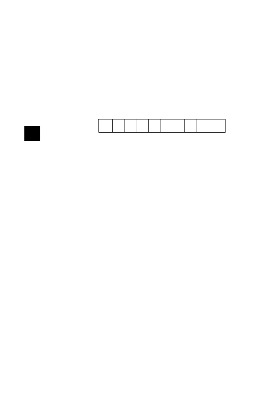
Address
bit 7
bit 6
bit 5
bit 4
bit 3
bit 2
bit 1
bit 0
State
on reset
Output compare 2 high (OCR2H)
$0026
Undened
Output compare 2 low (OCR2L)
$0027
Undened
TPG
64
05F32Book Page 12 Tuesday, June 8, 1999 7:55 am
相關(guān)PDF資料 |
PDF描述 |
|---|---|
| MC68HC705H12 | 8-BIT, EEPROM, 2 MHz, MICROCONTROLLER, PQCC52 |
| MC68HC705J1AVDWR2 | 8-BIT, OTPROM, 2.1 MHz, MICROCONTROLLER, PDSO20 |
| MC68HRC705J1ACDWR2 | 8-BIT, OTPROM, 2.1 MHz, MICROCONTROLLER, PDSO20 |
| MC68HSC705J1ACDWR2 | 8-BIT, OTPROM, 2.1 MHz, MICROCONTROLLER, PDSO20 |
| MC68HRC705J1ADWR2 | 8-BIT, OTPROM, 2.1 MHz, MICROCONTROLLER, PDSO20 |
相關(guān)代理商/技術(shù)參數(shù) |
參數(shù)描述 |
|---|---|
| MC68HC05F32CPU | 制造商:FREESCALE 制造商全稱:Freescale Semiconductor, Inc 功能描述:a member of the M68HC05 family of HCMOS |
| MC68HC05F32FU | 制造商:FREESCALE 制造商全稱:Freescale Semiconductor, Inc 功能描述:a member of the M68HC05 family of HCMOS |
| MC68HC05F32PU | 制造商:FREESCALE 制造商全稱:Freescale Semiconductor, Inc 功能描述:a member of the M68HC05 family of HCMOS |
| MC68HC05F4 | 制造商:MOTOROLA 制造商全稱:Motorola, Inc 功能描述:MECHANICAL DATA |
| MC68HC05F5 | 制造商:FREESCALE 制造商全稱:Freescale Semiconductor, Inc 功能描述:HCMOS Microcontroller Unit |
發(fā)布緊急采購,3分鐘左右您將得到回復(fù)。