- 您現(xiàn)在的位置:買賣IC網(wǎng) > PDF目錄369901 > MC44825D (MOTOROLA INC) TV AND VCR PLL TUNING CIRCUITS WITH 1.3 GHz PRESCALER AND I2C BUS PDF資料下載
參數(shù)資料
| 型號: | MC44825D |
| 廠商: | MOTOROLA INC |
| 元件分類: | XO, clock |
| 英文描述: | TV AND VCR PLL TUNING CIRCUITS WITH 1.3 GHz PRESCALER AND I2C BUS |
| 中文描述: | PLL FREQUENCY SYNTHESIZER, 1300 MHz, PDSO16 |
| 封裝: | PLASTIC, SO-16 |
| 文件頁數(shù): | 5/8頁 |
| 文件大?。?/td> | 158K |
| 代理商: | MC44825D |
MC44824/25
5
MOTOROLA ANALOG IC DEVICE DATA
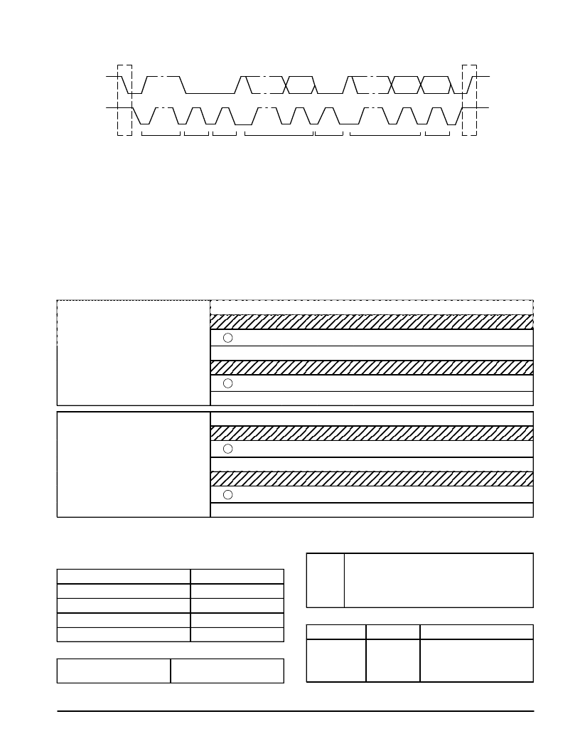
Figure 3. Complete Data Transfer Process
SDA
SCL
S
P
1–7
8
9
1–7
8
9
1–7
8
9
STA
ADDRESS
CA
R/W
ACK
DATA
ACK
DATA
ACK
STO
Figure 4 shows the five bytes of information that are
needed for circuit operation: there is the chip address, two
bytes of control and band information and two bytes of
frequency information.
After the chip address, two or four data bytes may be
received: if three data bytes are received, the third data byte
is ignored.
If five or more data bytes are received, the fifth and
following data bytes are ignored and the last acknowledge
pulse is sent at the end of the fourth data byte.
The first and the third data bytes contain a function bit
which allows the IC to distinguish between frequency
information and control plus band information.
Frequency information is preceded by a Logic “0”. If the
function bit is Logic “1” the two following bytes contain control
and band information. The first data byte, shifted after the
chip address, may be byte CO or byte FM.
The two permissible bus protocols with five bytes are
shown in Figure 4.
Figure 4. Definition of Bytes
CA_Chip Address
ééééééééééééééééééééééé
ééééééééééééééééééééééé
1
T14
T13
T12
T11
CO_Information
T10
T9
T8
ACK
BA_Band Information
ééééééééééééééééééééééé
ééééééééééééééééééééééé
0
N14
N13
N12
N11
FM_Frequency Information
N10
N9
N8
ACK
FL_Frequency Information
N7
N6
N5
N4
N3
N2
N1
N0
ACK
CA_Chip Address
1
1
0
0
0
0/1
0/1
0
ACK
ééééééééééééééééééééééé
ééééééééééééééééééééééé
FM_Frequency Information
FL_Frequency Information
N7
N6
N5
N4
N3
N2
N1
N0
ACK
ééééééééééééééééééééééé
ééééééééééééééééééééééé
CO_Information
BA_Band Information
B7
X
X
B4*
X
B2
B1
B0*
ACK
* B0 and B4 are only available on MC44825. On MC44824 this data is random.
Chip Address
The chip address is programmable by Pin 7 (8), CA.
CA – Pin 7 (8)
Address (HEX.)
Gnd to 0.1 VCC1
Open or 0.2 VCC1 to 0.3 VCC1
0.4 VCC1 to 0.7 VCC1
0.8 VCC1 to 1.1 VCC1
C0
C2
C4
C6
Bits B0, B1, B2, B4, B7: Control the Band Buffers
B0, B1, B2, B4, B7 = 0
B0, B1, B2, B4, B7
= 1
Buffer “Off”
Buffer “On”
Bit T8: Controls the Output of the Operational Amplifier
T8 = 0
Normal Operation
Operational Amplifier Active
Output State of Operational Amplifier Switched “Off”,
Output Pulls High Through an External Pull–Up
Resistor
T8
= 1
Bits T9, T12: Control the Phase Comparator
T9
T12
1
1
0
0
1
Function
0
1
0
Normal Operation
High Impedance
Upper Source “On” Only
Lower Source “On” Only
相關(guān)PDF資料 |
PDF描述 |
|---|---|
| MC44826D | TV AND VCR I2C PLL TUNING CIRCUIT WITH 1.3 GHz PRESCALER AND MIX/OSC DECODER |
| MC44827BDTB | LOW-POWER PLL TUNING CIRCUIT |
| MC44827 | LOW-POWER PLL TUNING CIRCUIT |
| MC44827DTB | LOW-POWER PLL TUNING CIRCUIT |
| MC44829D | TV AND VCR I2C PLL TUNING CIRCUIT WITH 1.3 GHz PRESCALER AND MIX/OSC DECODER |
相關(guān)代理商/技術(shù)參數(shù) |
參數(shù)描述 |
|---|---|
| MC44826D | 制造商:MOTOROLA 制造商全稱:Motorola, Inc 功能描述:TV AND VCR I2C PLL TUNING CIRCUIT WITH 1.3 GHz PRESCALER AND MIX/OSC DECODER |
| MC44827 | 制造商:MOTOROLA 制造商全稱:Motorola, Inc 功能描述:LOW-POWER PLL TUNING CIRCUIT |
| MC44827BDTB | 制造商:MOTOROLA 制造商全稱:Motorola, Inc 功能描述:LOW-POWER PLL TUNING CIRCUIT |
| MC44827DTB | 制造商:Rochester Electronics LLC 功能描述:- Bulk 制造商:Motorola Inc 功能描述: |
| MC44829 | 制造商:MOTOROLA 制造商全稱:Motorola, Inc 功能描述:TV AND VCR I2C PLL TUNING CIRCUIT WITH 1.3 GHz PRESCALER AND MIX/OSC DECODER |
發(fā)布緊急采購,3分鐘左右您將得到回復(fù)。