- 您現(xiàn)在的位置:買賣IC網(wǎng) > PDF目錄371034 > MC34270FB (MOTOROLA INC) Single Output LDO, 250mA, Fixed(3.0V), Low Noise, Fast Transient Response 5-SOT-23 -40 to 85 PDF資料下載
參數(shù)資料
| 型號(hào): | MC34270FB |
| 廠商: | MOTOROLA INC |
| 元件分類: | 穩(wěn)壓器 |
| 英文描述: | Single Output LDO, 250mA, Fixed(3.0V), Low Noise, Fast Transient Response 5-SOT-23 -40 to 85 |
| 中文描述: | 0.5 A DUAL SWITCHING CONTROLLER, 700 kHz SWITCHING FREQ-MAX, PQFP32 |
| 封裝: | PLASTIC, QFP-32 |
| 文件頁(yè)數(shù): | 1/12頁(yè) |
| 文件大?。?/td> | 364K |
| 代理商: | MC34270FB |
E
Device
Operating
Temperature Range
Package
SEMICONDUCTOR
TECHNICAL DATA
LIQUID CRYSTAL DISPLAY
AND BACKLIGHT
INTEGRATED CONTROLLER
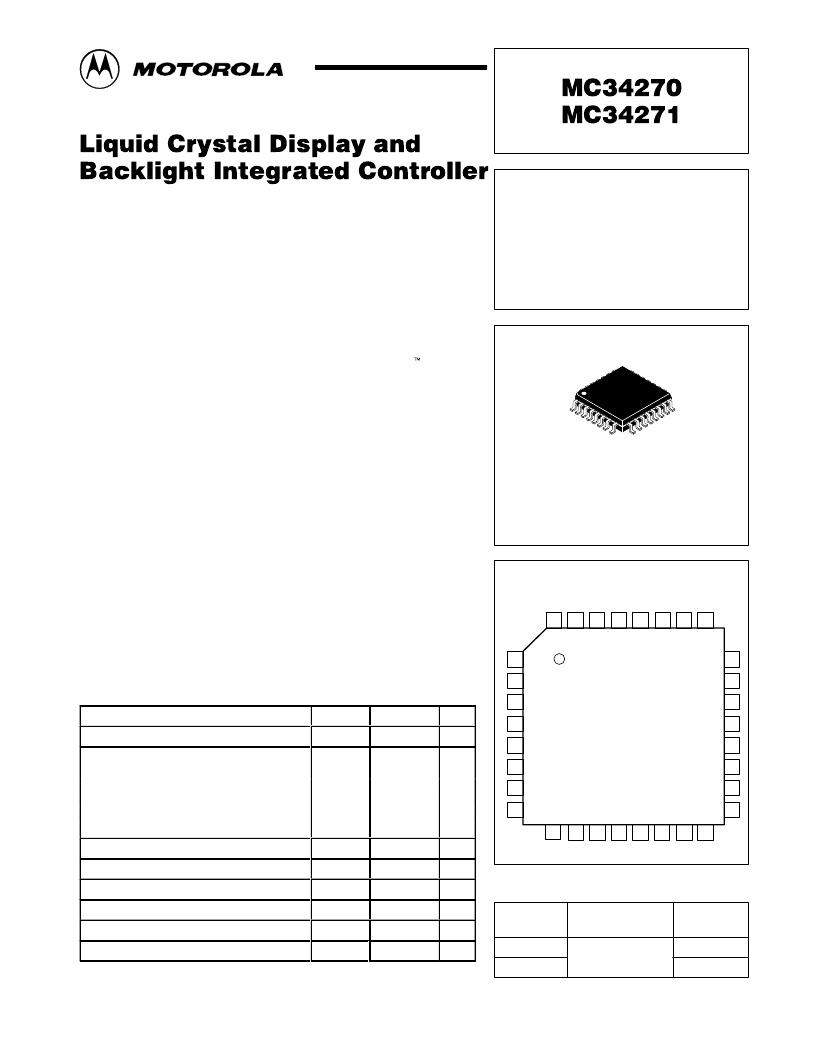
ORDERING INFORMATION
MC34270FB
MC34271FB
TA = 0
°
to +70
°
C
QFP–32
QFP–32
FB SUFFIX
PLASTIC PACKAGE
CASE 873
1
32
PIN CONNECTIONS
Order this document by MC34270/D
32
1
DS1
Ref1
FB1
Comp1
SS1
S1
D1
Drv1
DS2
Ref2
FB2
Comp2
SS2
S2
D2
VB
S
S
T
G
A
V
E
9
M
10
D
11
3
13
V
12
V
14
V
15
V
16
E
31
30
29
27
28
26
25
1
24
23
22
21
20
19
18
17
2
3
4
5
6
7
8
1
MOTOROLA ANALOG IC DEVICE DATA
The MC34270 and MC34271 are low power dual switching voltage
regulators, specifically designed for handheld and laptop applications, to
provide several regulated output voltages using a minimum of external parts.
Two uncommitted switching regulators feature a very low standby bias
current of 5.0
μ
A, and an operating current of 7.0 mA capable of supplying
output currents in excess of 200 mA.
Both devices have three additional features. The first is an ELD Output
that can be used to drive a backlight or a liquid crystal display. The ELD
output frequency is the clock divided by 256. The second feature allows
four additional output bias voltages, in specific proportions to VB, one of the
switching regulated output voltages. It allows use of mixed logic circuitry and
provides a voltage bias for N–Channel load control MOSFETs . The third
feature is an Enable input that allows a logic level signal to turn–“off” or
turn–“on” both switching regulators.
Due to the low bias current specifications, these devices are ideally suited
for battery powered computer, consumer, and industrial equipment where an
extension of useful battery life is desirable.
MC34270 and MC34271 Features:
Low Standby Bias Current of 5.0
μ
A
Uncommitted Switching Regulators Allow Both Positive and Negative
Supply Voltages
Logic Enable Allows Microprocessor Control of All Outputs
Synchronizable to External Clock
Mode Commandable for ELD and LCD Interface
Frequency Synchronizable
Auxiliary Output Bias Voltages Enable Load Control via N–Channel FETs
MOSFET is a trademark of Motorola, Inc.
MAXIMUM RATINGS
(TA = 25
°
C, unless otherwise noted.)
áááááááááááááááááááá
áááááááááááááááááááá
á
áááááááááááááááááá
Thermal Resistance, Junction–to–Ambient
Thermal Resistance, Junction–to–Case
ááá
ááááááááááá
Thermal Characteristics
Maximum Power Dissipation
á
áá
PD
ááá
1.43
á
á
W
á
R
θ
JA
R
θ
JC
VSL
VLF
TJ
TA
Tstg
100
60
°
C/W
°
C/W
áááááááááááááááááááá
áááááááááááááááááááá
áááááááááááááááááááá
á
Output #1 and #2 Switch Current
500
mA
Output #1 and #2 “Off”–State Voltage
áá
60
Vdc
áááááááááááááááááááá
Feedback Enable MOSFETs “Off”–State Voltage
20
Vdc
Operating Junction Temperature
125
°
C
áááááááááááááááááááá
Operating Ambient Temperature
0 to +70
°
C
áááááááááááááááááááá
ááááááááááá
á
Storage Temperature Range
ááá
á
á
á
°
C
Motorola, Inc. 1996
Rev 1
相關(guān)PDF資料 |
PDF描述 |
|---|---|
| MC3447 | BIDIRECTIONAL INSTRUMENTATION BUS(GPIB) TRANSCEIVER |
| MC3447P3 | BIDIRECTIONAL INSTRUMENTATION BUS(GPIB) TRANSCEIVER |
| MC3447P | BIDIRECTIONAL INSTRUMENTATION BUS(GPIB) TRANSCEIVER |
| MC3447L | BIDIRECTIONAL INSTRUMENTATION BUS(GPIB) TRANSCEIVER |
| MC3448AL | QUAD THREE-STATE BUS TRANSCEIVER WITH TERMINATION NETWORKS |
相關(guān)代理商/技術(shù)參數(shù) |
參數(shù)描述 |
|---|---|
| MC34271FB | 制造商:Rochester Electronics LLC 功能描述:- Bulk |
| MC34280FTB | 制造商:ON Semiconductor 功能描述: |
| MC3430 | 制造商:mCube 功能描述: |
| MC3430P | 制造商:Motorola Inc 功能描述: |
| MC34311 | 制造商:SPC Multicomp 功能描述:HEADER R/ANGLE 2WAY 制造商:SPC Multicomp 功能描述:HEADER, R/ANGLE, 2WAY 制造商:SPC Multicomp 功能描述:WIRE-BOARD CONNECTOR, RCPT, 2POS, 4.2MM; Series:2261(5561); Pitch Spacing:4.2mm; Contact Termination:Through Hole Right Angle; No. of Contacts:2; No. of Rows:2; Connector Mounting:PCB; Gender:Receptacle; Contact Material:Copper Alloy;RoHS Compliant: Yes |
發(fā)布緊急采購(gòu),3分鐘左右您將得到回復(fù)。