- 您現(xiàn)在的位置:買賣IC網(wǎng) > PDF目錄385567 > MC34262P (ON SEMICONDUCTOR) POWER FACTOR CONTROLLERS PDF資料下載
參數(shù)資料
| 型號: | MC34262P |
| 廠商: | ON SEMICONDUCTOR |
| 元件分類: | 穩(wěn)壓器 |
| 英文描述: | POWER FACTOR CONTROLLERS |
| 中文描述: | 0.5 A POWER FACTOR CONTROLLER, PDIP8 |
| 封裝: | PLASTIC, DIP-8 |
| 文件頁數(shù): | 8/16頁 |
| 文件大小: | 393K |
| 代理商: | MC34262P |
MC34262 MC33262
8
MOTOROLA ANALOG IC DEVICE DATA
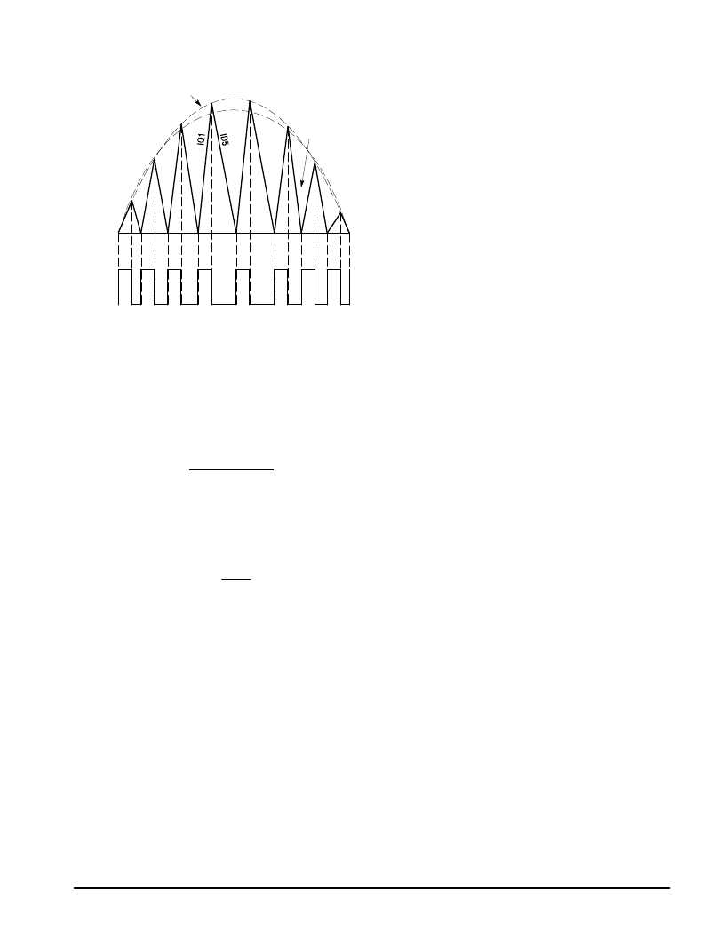
Figure 18. Inductor Current and MOSFET
Gate Voltage Waveforms
Inductor Current
Average
MOSFET
Q1
On
Off
0
Peak
Current Sense Comparator and RS Latch
The Current Sense Comparator RS Latch configuration
used ensures that only a single pulse appears at the Drive
Output during a given cycle. The inductor current is
converted to a voltage by inserting a ground–referenced
sense resistor R7 in series with the source of output switch
Q1. This voltage is monitored by the Current Sense Input and
compared to a level derived from the Multiplier output. The
peak inductor current under normal operating conditions is
controlled by the threshold voltage of Pin 4 where:
Pin 4 Threshold
R7
IL(pk ) =
Abnormal operating conditions occur during preconverter
startup at extremely high line or if output voltage sensing is
lost. Under these conditions, the Multiplier output and Current
Sense threshold will be internally clamped to 1.5 V.
Therefore, the maximum peak switch current is limited to:
1.5 V
R7
Ipk(max) =
An internal RC filter has been included to attenuate any
high frequency noise that may be present on the current
waveform. This filter helps reduce the ac line current
distortion especially near the zero crossings. With the
component values shown in Figure 20, the Current Sense
Comparator threshold, at the peak of the haversine varies
from 1.1 V at 90 Vac to 100 mV at 268 Vac. The Current
Sense Input to Drive Output turn–off propagation delay is
typically less than 200 ns.
Timer
A watchdog timer function was added to the IC to eliminate
the need for an external oscillator when used in stand–alone
applications. The Timer provides a means to automatically
start or restart the preconverter if the Drive Output has been
off for more than 620
μ
s after the inductor current reaches
zero. The restart time delay versus temperature is shown in
Figure 8.
Undervoltage Lockout and Quickstart
An Undervoltage Lockout comparator has been
incorporated to guarantee that the IC is fully functional before
enabling the output stage. The positive power supply terminal
(VCC) is monitored by the UVLO comparator with the upper
threshold set at 13 V and the lower threshold at 8.0 V. In the
stand–by mode, with VCC at 7.0 V, the required supply current
is less than 0.4 mA. This large hysteresis and low startup
current allow the implementation of efficient bootstrap startup
techniques, making these devices ideally suited for wide
input range off–line preconverter applications. An internal
36 V clamp has been added from VCC to ground to protect
the IC and capacitor C4 from an overvoltage condition. This
feature is desirable if external circuitry is used to delay the
startup of the preconverter. The supply current, startup, and
operating voltage characteristics are shown in Figures 13
and 14.
A Quickstart circuit has been incorporated to optimize
converter startup. During initial startup, compensation
capacitor C1 will be discharged, holding the error amp output
below the Multiplier threshold. This will prevent Drive Output
switching and delay bootstrapping of capacitor C4 by diode
D6. If Pin 2 does not reach the multiplier threshold before C4
discharges below the lower UVLO threshold, the converter
will “hiccup” and experience a significant startup delay. The
Quickstart circuit is designed to precharge C1 to 1.7 V, Figure
7. This level is slightly below the Pin 2 Multiplier threshold,
allowing immediate Drive Output switching and bootstrap
operation when C4 crosses the upper UVLO threshold.
Drive Output
The MC34262/MC33262 contain a single totem–pole
output stage specifically designed for direct drive of power
MOSFETs. The Drive Output is capable of up to
±
500 mA
peak current with a typical rise and fall time of 50 ns with a
1.0 nF load. Additional internal circuitry has been added to
keep the Drive Output in a sinking mode whenever the
Undervoltage Lockout is active. This characteristic eliminates
the need for an external gate pull–down resistor. The
totem–pole output has been optimized to minimize
cross–conduction current during high speed operation. The
addition of two 10
resistors, one in series with the source
output transistor and one in series with the sink output
transistor, helps to reduce the cross–conduction current and
radiated noise by limiting the output rise and fall time. A 16 V
clamp has been incorporated into the output stage to limit the
high state VOH. This prevents rupture of the MOSFET gate
when VCC
exceeds 20 V.
相關(guān)PDF資料 |
PDF描述 |
|---|---|
| MC34262 | Power Factor Controllers(功率因數(shù)控制器) |
| MC34280 | Power Supply & Management IC for Handheld Electronic Products(用于手提電子產(chǎn)品的電源管理芯片) |
| MC3479 | Stepper Motor Driver(步進電機驅(qū)動器) |
| MC44BC375 | PLL Tuned VHF Audio/ Video High Integration Modulator ICs |
| MC44BC375J | PLL Tuned VHF Audio/ Video High Integration Modulator ICs |
相關(guān)代理商/技術(shù)參數(shù) |
參數(shù)描述 |
|---|---|
| MC34262PG | 功能描述:功率因數(shù)校正 IC Critical Mode PFC w/OVP RoHS:否 制造商:Fairchild Semiconductor 開關(guān)頻率:300 KHz 最大功率耗散: 最大工作溫度:+ 125 C 安裝風格:SMD/SMT 封裝 / 箱體:SOIC-8 封裝:Reel |
| MC34262PG | 制造商:ON Semiconductor 功能描述:Power Supply IC |
| MC34268D | 功能描述:低壓差穩(wěn)壓器 - LDO 2.85V 800mA SCSI-2 RoHS:否 制造商:Texas Instruments 最大輸入電壓:36 V 輸出電壓:1.4 V to 20.5 V 回動電壓(最大值):307 mV 輸出電流:1 A 負載調(diào)節(jié):0.3 % 輸出端數(shù)量: 輸出類型:Fixed 最大工作溫度:+ 125 C 安裝風格:SMD/SMT 封裝 / 箱體:VQFN-20 |
| MC34268DG | 功能描述:低壓差穩(wěn)壓器 - LDO 2.85V 800mA SCSI-3 Active Terminator RoHS:否 制造商:Texas Instruments 最大輸入電壓:36 V 輸出電壓:1.4 V to 20.5 V 回動電壓(最大值):307 mV 輸出電流:1 A 負載調(diào)節(jié):0.3 % 輸出端數(shù)量: 輸出類型:Fixed 最大工作溫度:+ 125 C 安裝風格:SMD/SMT 封裝 / 箱體:VQFN-20 |
| MC34268DR2 | 功能描述:低壓差穩(wěn)壓器 - LDO 2.85V 800mA SCSI-4 RoHS:否 制造商:Texas Instruments 最大輸入電壓:36 V 輸出電壓:1.4 V to 20.5 V 回動電壓(最大值):307 mV 輸出電流:1 A 負載調(diào)節(jié):0.3 % 輸出端數(shù)量: 輸出類型:Fixed 最大工作溫度:+ 125 C 安裝風格:SMD/SMT 封裝 / 箱體:VQFN-20 |
發(fā)布緊急采購,3分鐘左右您將得到回復。