- 您現(xiàn)在的位置:買賣IC網(wǎng) > PDF目錄382304 > MC33765DTB (ON SEMICONDUCTOR) Very Low Dropout/Ultra Low Noise 5 Outputs Voltage Regulator PDF資料下載
參數(shù)資料
| 型號: | MC33765DTB |
| 廠商: | ON SEMICONDUCTOR |
| 元件分類: | 基準(zhǔn)電壓源/電流源 |
| 英文描述: | Very Low Dropout/Ultra Low Noise 5 Outputs Voltage Regulator |
| 中文描述: | FIVE OUTPUT, FIXED POSITIVE LDO REGULATOR, PDSO16 |
| 封裝: | LEAD FREE, TSSOP-16 |
| 文件頁數(shù): | 10/16頁 |
| 文件大小: | 287K |
| 代理商: | MC33765DTB |

MC33765
http://onsemi.com
10
DEFINITIONS
Load Regulation
– The change in output voltage for a
change in load current at constant chip temperature.
Dropout Voltage
– The input/output differential at which
the regulator output no longer maintains regulation against
further reductions in input voltage. Measured when the
output drops 100 mV below its nominal value (which is
measured at 1.0 V differential input/output), dropout voltage
is affected by junction temperature, load current and
minimum input supply requirements.
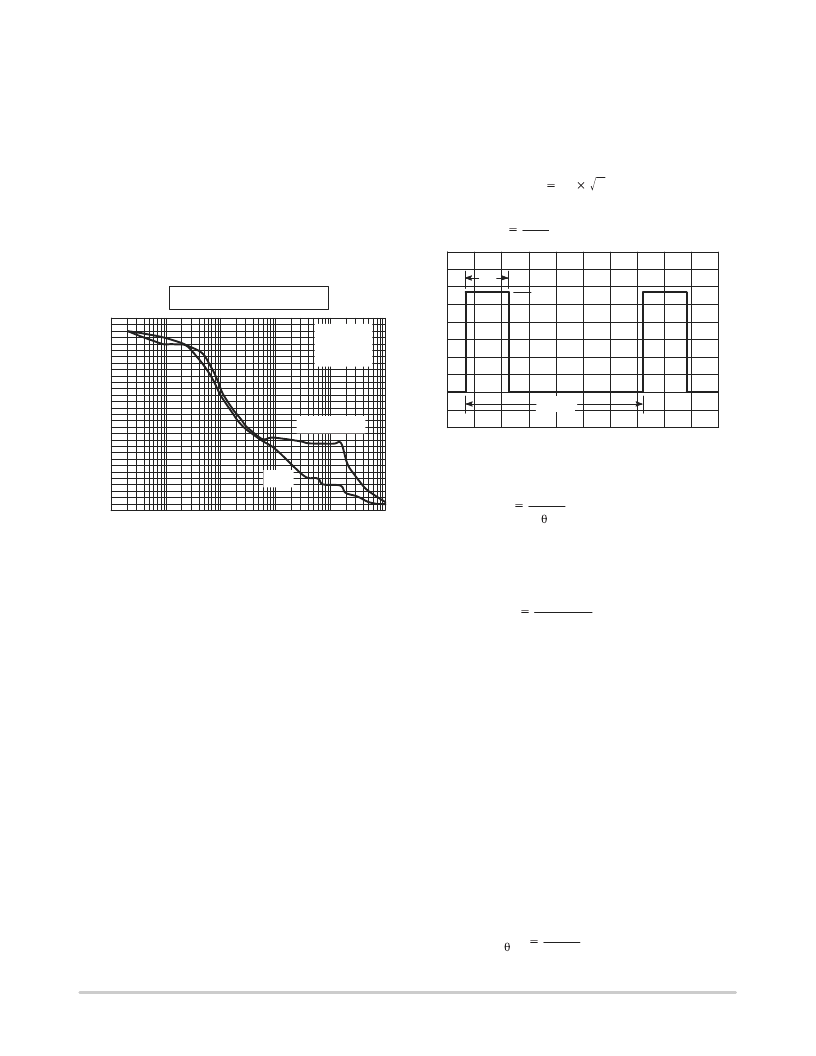
Output Noise Voltage
– The RMS AC voltage at the
output with a constant load and no input ripple, measured
over a specified frequency range.
n
10
100
10000
0
100
Frequency (Hz)
1000
150
50
300
OUT1, 2, 3, 4, 5
200
250
100000
1000000
OUT3
MC33765 Output noise performances
Vin = 3.6V
Iout = typical
Cbyp = 10nF
Maximum Power Dissipation
– The maximum total
dissipation for which the regulator will operate within
specifications.
Quiescent Current
– Current which is used to operate the
regulator chip with no load current.
Line Regulation
– The change in input voltage for a
change in the input voltage. The measurement is made under
conditions of low dissipation or by using pulse techniques
such that the average chip temperature is not significantly
affected.
Thermal Protection
– Internal thermal shutdown
circuitry is provided to protect the integrated circuit in the
event that the maximum junction temperature is exceeded.
When activated, typically 160
°
C, the regulator turns off.
This feature is provided to prevent catastrophic failures from
accidental overheating.
Maximum Package Power Dissipation and RMS
Current
– The maximum package power dissipation is the
power dissipation level at which the junction temperature
reaches its maximum value i.e. 125
°
C. The junction
temperature is rising while the difference between the input
power (VCC X ICC) and the output power (Vout X Iout) is
increasing.
As MC33765 device exhibits five independent outputs
Iout is specified as the maximum RMS current combination
of the five output currents.
As the device can be switched ON/OFF through
independent Enable (ON/OFF pin) or Common Enable, the
output signal could be, for example, a square wave. Let’s
assume that the device is ON during TON on a signal period
T. The RMS current will be given by:
IoutRMS
IP
D
D
TON
T
where
Ton
Ip
T, period
Depending on ambient temperature, it is possible to
calculate the maximum power dissipation and so the
maximum RMS current as following:
TJ– TA
RJA
The maximum operating junction temperature TJ is
specified at 125
°
C, if TA = 25
°
C, then PD = 700 mW. By
neglecting the quiescent current, the maximum power
dissipation can be expressed as:
PD
VCC– Vout
So that in the more drastic conditions:
VCC = 5.3 V, Vout = 2.7 V then the maximum RMS value of
Iout is 269 mA.
The maximum power dissipation supported by the device
is a lot increased when using appropriate application design.
Mounting pad configuration on the PCB, the board material
and also the ambient temperature are affected the rate of
temperature rise. It means that when the IC has good thermal
conductivity through PCB, the junction temperature will be
“l(fā)ow” even if the power dissipation is great.
The thermal resistance of the whole circuit can be
evaluated by deliberately activating the thermal shutdown
of the circuit (by increasing the output current or raising the
input voltage for example).
Then you can calculate the power dissipation by subtracting
the output power from the input power. All variables are then
well known: power dissipation, thermal shutdown temperature
(160
°
C for MC33765) and ambient temperature.
TJ– TA
PD
Pd
Iout
RJA
相關(guān)PDF資料 |
PDF描述 |
|---|---|
| MC33765DTBR2 | Very Low Dropout/Ultra Low Noise 5 Outputs Voltage Regulator |
| MC33887 | 5.0 A H-Bridge with Load Current Feedback |
| MC33887DH | 5.0 A H-Bridge with Load Current Feedback |
| MC33887DHR2 | 5.0 A H-Bridge with Load Current Feedback |
| MC33887DWB | 5.0 A H-Bridge with Load Current Feedback |
相關(guān)代理商/技術(shù)參數(shù) |
參數(shù)描述 |
|---|---|
| MC33765DTBG | 功能描述:低壓差穩(wěn)壓器 - LDO 5 Output Ultra LDO Low Noise Regulator RoHS:否 制造商:Texas Instruments 最大輸入電壓:36 V 輸出電壓:1.4 V to 20.5 V 回動電壓(最大值):307 mV 輸出電流:1 A 負(fù)載調(diào)節(jié):0.3 % 輸出端數(shù)量: 輸出類型:Fixed 最大工作溫度:+ 125 C 安裝風(fēng)格:SMD/SMT 封裝 / 箱體:VQFN-20 |
| MC33765DTBR2 | 功能描述:低壓差穩(wěn)壓器 - LDO 5 Output Ultra LDO RoHS:否 制造商:Texas Instruments 最大輸入電壓:36 V 輸出電壓:1.4 V to 20.5 V 回動電壓(最大值):307 mV 輸出電流:1 A 負(fù)載調(diào)節(jié):0.3 % 輸出端數(shù)量: 輸出類型:Fixed 最大工作溫度:+ 125 C 安裝風(fēng)格:SMD/SMT 封裝 / 箱體:VQFN-20 |
| MC33765DTBR2G | 功能描述:低壓差穩(wěn)壓器 - LDO 5 Output Ultra LDO Low Noise Regulator RoHS:否 制造商:Texas Instruments 最大輸入電壓:36 V 輸出電壓:1.4 V to 20.5 V 回動電壓(最大值):307 mV 輸出電流:1 A 負(fù)載調(diào)節(jié):0.3 % 輸出端數(shù)量: 輸出類型:Fixed 最大工作溫度:+ 125 C 安裝風(fēng)格:SMD/SMT 封裝 / 箱體:VQFN-20 |
| MC33780EG | 功能描述:IC DBUS MASTER DUAL DIFF 16-SOIC RoHS:是 類別:集成電路 (IC) >> 專用 IC 系列:* 產(chǎn)品培訓(xùn)模塊:Lead (SnPb) Finish for COTS Obsolescence Mitigation Program 標(biāo)準(zhǔn)包裝:1 系列:- 類型:調(diào)幀器 應(yīng)用:數(shù)據(jù)傳輸 安裝類型:表面貼裝 封裝/外殼:400-BBGA 供應(yīng)商設(shè)備封裝:400-PBGA(27x27) 包裝:散裝 |
| MC33780EGR2 | 功能描述:IC DBUS MASTER DUAL DIFF 16-SOIC RoHS:是 類別:集成電路 (IC) >> 專用 IC 系列:* 產(chǎn)品培訓(xùn)模塊:Lead (SnPb) Finish for COTS Obsolescence Mitigation Program 標(biāo)準(zhǔn)包裝:1 系列:- 類型:調(diào)幀器 應(yīng)用:數(shù)據(jù)傳輸 安裝類型:表面貼裝 封裝/外殼:400-BBGA 供應(yīng)商設(shè)備封裝:400-PBGA(27x27) 包裝:散裝 |
發(fā)布緊急采購,3分鐘左右您將得到回復(fù)。