- 您現(xiàn)在的位置:買賣IC網(wǎng) > PDF目錄369901 > MC3374 (Motorola, Inc.) LOW VOLTAGE SINGLE CONVERSION FM RECEIVER PDF資料下載
參數(shù)資料
| 型號: | MC3374 |
| 廠商: | Motorola, Inc. |
| 英文描述: | LOW VOLTAGE SINGLE CONVERSION FM RECEIVER |
| 中文描述: | 低電壓單次轉(zhuǎn)換調(diào)頻接收機 |
| 文件頁數(shù): | 3/8頁 |
| 文件大?。?/td> | 237K |
| 代理商: | MC3374 |

MC3374
3
MOTOROLA ANALOG IC DEVICE DATA
ELECTRICAL CHARACTERISTICS (continued)
(VCC = 1.3 V, fo = 10.7 MHz, fmod = 1.0 kHz, Deviation = 3.0 kHz, TA
= 25
°
C, Test Circuit of Figure 1, unless otherwise noted.)
Characteristic
Pin
Min
Typ
Max
Unit
COMPARATOR
Minimum Input for Triggering (RL = 100 k
)
Maximum Input Frequency (RL = 100 k
)
Rise Time (10–90%; RL = 100 k
)
Fall Time (90–10%; RL = 100 k
)
LOW BATTERY DETECTOR
Low Battery Trip Point
13
–
7.0
–
mVrms
13
–
25
–
kHz
μ
s
μ
s
14
–
5.0
–
14
–
0.4
–
19
–
1.2
–
Vdc
Low Battery Output – VCC = 0.9 V
Low Battery Output
– VCC = 1.3 V
VOLTAGE REGULATOR
Regulated Output (see Figure 4)
20
20
–
–
0.2
VCC
–
–
Vdc
17
0.95
1.07
1.15
Vdc
Source Capability
17
–
–
3.0
mA
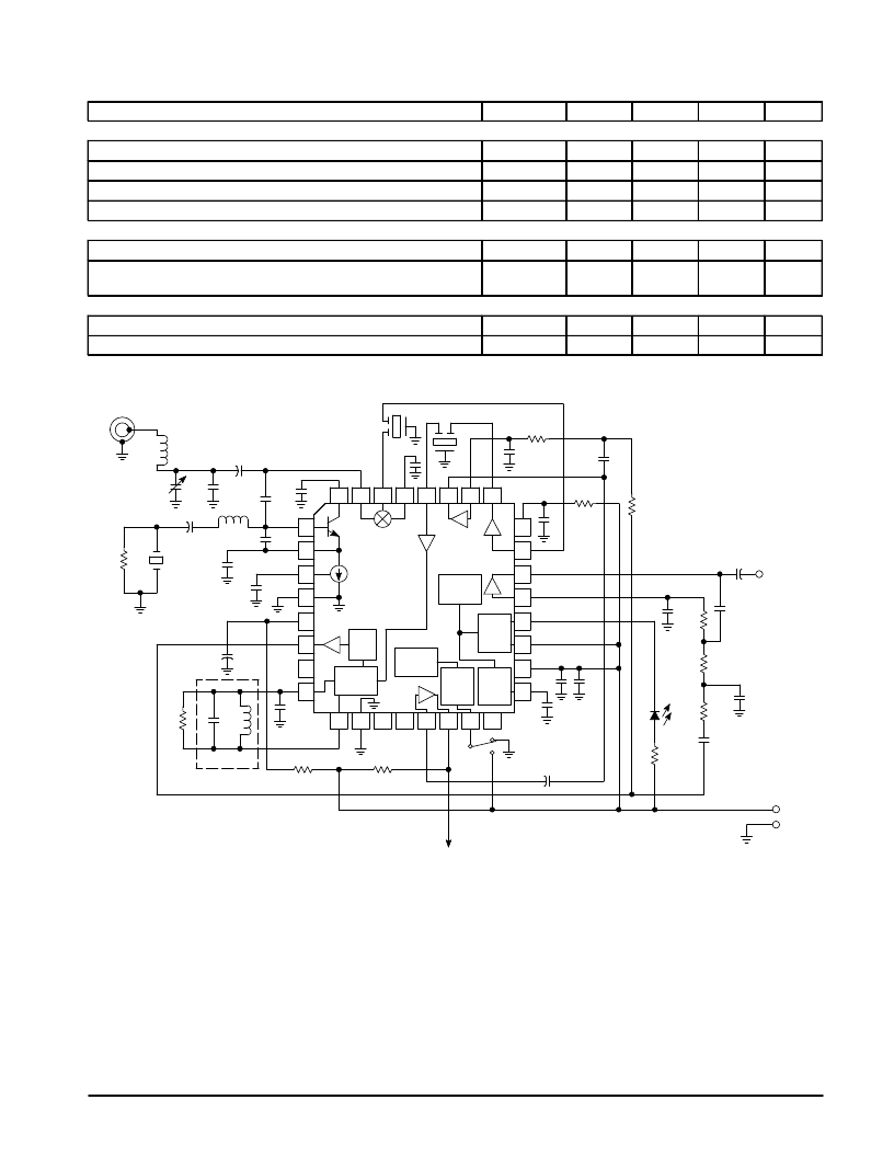
Figure 1. MC3374 Pager IF Application Circuit
NOTES:
1.FL1 and FL2 are 455 kHz ceramic bandpass filters, which should
have input and output impedances of 1.5 k
to 2.0 k
. Suggested
part numbers are MuRata CFU455X or CFW455x – the ‘X’ suffix
denotes bandwidth.
2.LC1 is a 455 kHz LC resonator. Recommended part numbers are
Toko America RMC2A6597HM or 5SVLC–0637BGT (smaller).
The evaluation board layout shown provides for use of either
resonator. Ceramic discriminator elements cannot be used with
the MC3374 due to their low input impedance. The damping
resistor value can be raised to increase the recovered audio or
lowered to increase the quadrature detector’s bandwidth and
linearity – practical limits are approximately 27 k
to 75 k
.
Typically the quadrature detector’s bandwidth should match the
low IF filter’s bandwidth.
3.The data buffer is set up as a low–pass filter with a corner
frequency of approximately 200 Hz. The audio buffer is a
bandpass filter with corner frequencies of 300 Hz and 3.0 kHz.
The audio amplifier provides bass suppression.
4.CC1 and CC3 are RF coupling capacitors and should have
≤
20
impedance at the desired input and oscillator frequencies.
5.CC2 provides “l(fā)ight coupling” of the oscillator signal into the mixer,
and should have a 3.0 k
to 5.0 k
impedance at the desired
local oscillator frequency.
6.Capacitors labelled CB are bypass capacitors and should have
20
impedance at the desired RF and local oscillator frequencies.
7.The network of L1, C1 and C2 provides impedance matching of
the mixer input (nominally 3.0 k
shunted by 9.0 pF) to 50
at the
desired RF/IF input frequency. This will allow for bench testing of
the receiver from typical RF signal generators or radio service
monitors, but additional or different matching will be required to
maximize receiver sensitivity when used in conjunction with an
antenna, RF preamplifier or mixer.
1
2
3
4
5
6
7
8
24
23
22
21
20
19
18
17
32
31
30
29
28
27
26
25
9
10
11
12
13
14
15
16
RF Input
50
L1
CC1
CC2
C2
C1
L2
CC3
X
RD
C4
CB
CB
10
56 k
LC1
100
100 k
0.1
Data Output
Enable
Disable
0.1
10
1.0
4.7
–
330
0.1
39 k
180 k
0.01
FL2
FL1
CB
0.1
1.0
μ
F
3900 P
0.022
0.22
8.2 k
8.2 k
3.3 k
Audio
Output
VCC
VEE
MC3374
N.C. N.C.
C3
Low
Pass
Filter
Quadrature
Demodulator
Main
Current
Reference
Output
Buffer
Receiver
Enable
Voltage
Reference
Low
Battery
Detector
Voltage
Reference
Audio
Buffer
Data
Buffer
Mixer
2nd IF
1st IF
Comp.
RL
+
相關(guān)PDF資料 |
PDF描述 |
|---|---|
| MC34001BU | JFET Input Operational Amplifiers |
| MC34001U | JFET Input Operational Amplifiers |
| MC34062 | METER DPM LED 3.5DIGIT GREEN |
| MC34062P1 | PIN-PROGRAMMABLE OVERVOLTAGE SENSING CIRCUIT |
| MC35062 | PIN-PROGRAMMABLE OVERVOLTAGE SENSING CIRCUIT |
相關(guān)代理商/技術(shù)參數(shù) |
參數(shù)描述 |
|---|---|
| MC33742DW | 功能描述:網(wǎng)絡(luò)控制器與處理器 IC SBC-E-HS RoHS:否 制造商:Micrel 產(chǎn)品:Controller Area Network (CAN) 收發(fā)器數(shù)量: 數(shù)據(jù)速率: 電源電流(最大值):595 mA 最大工作溫度:+ 85 C 安裝風格:SMD/SMT 封裝 / 箱體:PBGA-400 封裝:Tray |
| MC33742DWR2 | 功能描述:網(wǎng)絡(luò)控制器與處理器 IC SBC-E-HS RoHS:否 制造商:Micrel 產(chǎn)品:Controller Area Network (CAN) 收發(fā)器數(shù)量: 數(shù)據(jù)速率: 電源電流(最大值):595 mA 最大工作溫度:+ 85 C 安裝風格:SMD/SMT 封裝 / 箱體:PBGA-400 封裝:Tray |
| MC33742EP | 功能描述:CAN 接口集成電路 SBC_ECAN_HS RoHS:否 制造商:Texas Instruments 類型:Transceivers 工作電源電壓:5 V 電源電流: 工作溫度范圍:- 40 C to + 85 C 封裝 / 箱體:SOIC-8 封裝:Tube |
| MC33742EPR2 | 功能描述:CAN 接口集成電路 SBC_ECAN_HS RoHS:否 制造商:Texas Instruments 類型:Transceivers 工作電源電壓:5 V 電源電流: 工作溫度范圍:- 40 C to + 85 C 封裝 / 箱體:SOIC-8 封裝:Tube |
| MC33742PEG | 功能描述:CAN 接口集成電路 SBC-E-HS-CAN RoHS:否 制造商:Texas Instruments 類型:Transceivers 工作電源電壓:5 V 電源電流: 工作溫度范圍:- 40 C to + 85 C 封裝 / 箱體:SOIC-8 封裝:Tube |
發(fā)布緊急采購,3分鐘左右您將得到回復(fù)。