- 您現(xiàn)在的位置:買賣IC網(wǎng) > PDF目錄371016 > MC145406DW (MOTOROLA INC) Ultra Low-Supply Current/Supply-Voltage Supervisory Circuits 6-SOT-23 -40 to 85 PDF資料下載
參數(shù)資料
| 型號: | MC145406DW |
| 廠商: | MOTOROLA INC |
| 元件分類: | 通用總線功能 |
| 英文描述: | Ultra Low-Supply Current/Supply-Voltage Supervisory Circuits 6-SOT-23 -40 to 85 |
| 中文描述: | LINE TRANSCEIVER, PDSO16 |
| 封裝: | SOG-16 |
| 文件頁數(shù): | 4/12頁 |
| 文件大小: | 155K |
| 代理商: | MC145406DW |
MC145406
4
MOTOROLA
Vin =
±
2 V
3
5
7
14
12
10
8
9
1
VDD
16
VCC
DI1
DI2
DI3
VSS
GND
Tx3
Tx2
Tx1
Rout =
Vin
I
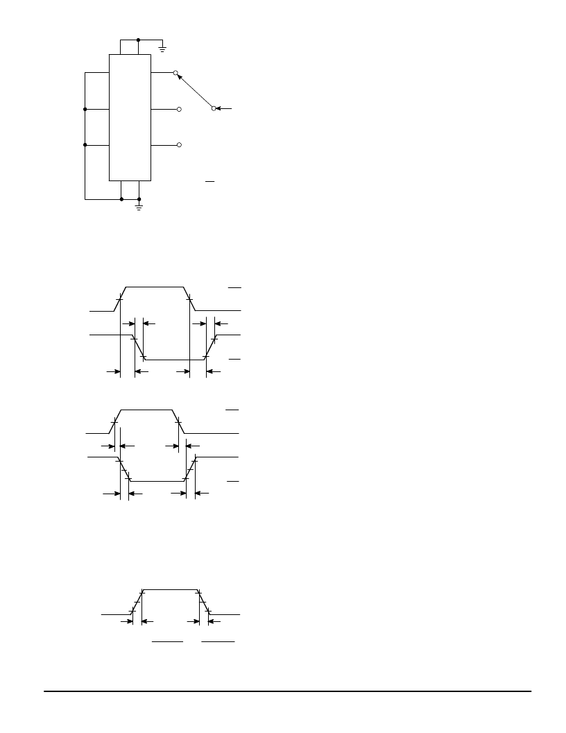
Figure 1. Power–Off Source Resistance (Drivers)
Figure 2. Switching Characteristics
Figure 3. Slew–Rate Characterization
DRIVERS
DI1–DI3
3 V
0 V
VOH
VOL
Tx1–Tx3
tPLH
tPHL
50%
tf
tr
10%
90%
RECEIVERS
Rx1–Rx3
DO1–DO3
+ 3 V
0 V
VOH
VOL
tPLH
tPHL
tf
tr
50%
DRIVERS
Tx1–Tx3
90%
50%
10%
3 V
– 3 V
3 V
– 3 V
tSHL
tSLH
SLEW RATE (SR) =– 3 V – (3 V)OR3 V – ( – 3 V)
tSLH
tSHL
PIN DESCRIPTIONS
VDD
Positive Power Supply (Pin 1)
The most positive power supply pin, which is typically + 5
to +
12V.
VSS
Negative Power Supply (Pin 8)
The most negative power supply pin, which is typically – 5
to –
12 V.
VCC
Digital Power Supply (Pin 16)
The digital supply pin, which is connected to the logic
power supply (maximum +
5.5 V). VCC
must
be less than
or equal to VDD.
GND
Ground (Pin 9)
Ground return pin is typically connected to the signal
ground pin of the EIA 232–E connector (Pin 7) as well as to
the logic power supply ground.
Rx1, Rx2, Rx3
Receive Data Input (Pins 2, 4, 6)
These are the EIA 232–E receive signal inputs whose
voltages can range from (VDD + 15 V) to (VSS – 15 V). A volt-
age between +
3 and (VDD + 15 V) is decoded as a space
and causes the corresponding DO pin to swing to ground (0
V); a voltage between – 3 and (VDD – 15 V) is decoded as a
mark and causes the DO pin to swing up to VCC. The actual
turn–on input switchpoint is typically biased at 1.8 V above
ground, and includes 800mV of hysteresis for noise rejec-
tion. The nominal input impedance is 5 k
. An open or
grounded input pin is interpreted as a mark, forcing the DO
pin to VCC.
DO1, DO2, DO3
Data Output (Pins 11, 13, 15)
These are the receiver digital output pins, which swing
from VCC to GND. A space on the Rx pin causes DO to pro-
duce a logic 0; a mark produces a logic 1. Each output pin is
capable of driving one LSTTL input load.
DI1, DI2, DI3
Data Input (Pins 10, 12,14)
These are the high–impedance digital input pins to the
drivers. TTL compatibility is accomplished by biasing the in-
put switchpoint at 1.4 V above GND. However, 5–V CMOS
compatibility is maintained as well. Input voltage levels on
these pins must be between VCC and GND.
Tx1, Tx2, Tx3
Transmit Data Output(Pins 3, 5, 7)
These are the EIA 232–E transmit signal output pins,
which swing toward VDD and VSS. A logic 1 at a DI input
causes the corresponding Tx output to swing toward VSS. A
logic 0 causes the output to swing toward VDD (the output
voltages will be slightly less than VDD or VSS depending upon
the output load). Output slew rates are limited to a maximum
of 30 V per
μ
s. When the MC145406 is off (VDD = VSS = VCC
= GND), the minimum output impedance is 300
.
相關(guān)PDF資料 |
PDF描述 |
|---|---|
| MC145406P | Ultra Low-Supply Current/Supply-Voltage Supervisory Circuits 6-SOT-23 -40 to 85 |
| MC145406SD | UltraLow-Supply Current/Supply-Voltage Supervisory Circuits 6-SOT-23 -40 to 85 |
| MC145407 | 5 Volt Only Driver/ Receiver(5V 驅(qū)動器/接收器) |
| MC145407DW | UltraLow-Supply Current/Supply-Voltage Supervisory Circuits 6-SOT-23 -40 to 85 |
| MC145407P | UltraLow-Supply Current/Supply-Voltage Supervisory Circuits 6-SOT-23 -40 to 85 |
相關(guān)代理商/技術(shù)參數(shù) |
參數(shù)描述 |
|---|---|
| MC145406DWR2 | 制造商:Rochester Electronics LLC 功能描述:- Bulk |
| MC145406F | 制造商:Rochester Electronics LLC 功能描述:3X3 RS232 TRANSCEIVER - Bulk |
| MC145406FEL | 制造商:Rochester Electronics LLC 功能描述:- Bulk |
| MC145406FR2 | 制造商:Rochester Electronics LLC 功能描述:- Bulk |
| MC145406N,602 | 功能描述:緩沖器和線路驅(qū)動器 TRIPLE DRVR/RECEIVER RS232-D/V.29 RoHS:否 制造商:Micrel 輸入線路數(shù)量:1 輸出線路數(shù)量:2 極性:Non-Inverting 電源電壓-最大:+/- 5.5 V 電源電壓-最小:+/- 2.37 V 最大工作溫度:+ 85 C 安裝風(fēng)格:SMD/SMT 封裝 / 箱體:MSOP-8 封裝:Reel |
發(fā)布緊急采購,3分鐘左右您將得到回復(fù)。