- 您現(xiàn)在的位置:買賣IC網(wǎng) > PDF目錄382296 > MC14049BFEL (ON SEMICONDUCTOR) Hex Buffer PDF資料下載
參數(shù)資料
| 型號(hào): | MC14049BFEL |
| 廠商: | ON SEMICONDUCTOR |
| 元件分類: | 通用總線功能 |
| 英文描述: | Hex Buffer |
| 中文描述: | 4000/14000/40000 SERIES, HEX 1-INPUT INVERT GATE, PDSO16 |
| 封裝: | PLASTIC, EIAJ, SOP-16 |
| 文件頁(yè)數(shù): | 1/8頁(yè) |
| 文件大小: | 205K |
| 代理商: | MC14049BFEL |

Semiconductor Components Industries, LLC, 2000
March, 2000 – Rev. 3
1
Publication Order Number:
MC14049UB/D
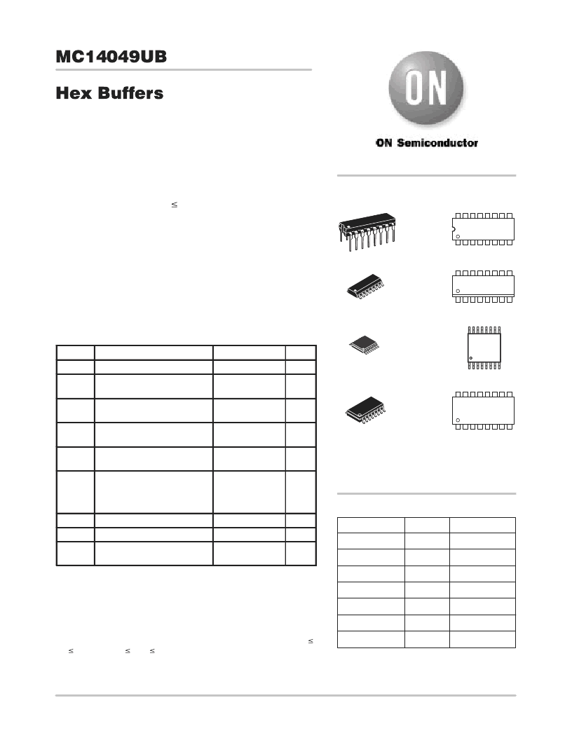
The MC14049UB hex inverter/buffer is constructed with MOS
P–channel and N–channel enhancement mode devices in a single
monolithic structure. This complementary MOS device finds primary
use where low power dissipation and/or high noise immunity is
desired. This device provides logic–level conversion using only one
supply voltage, V
DD
. The input–signal high level (V
IH
) can exceed the
V
DD
supply voltage for logic–level conversions. Two TTL/DTL
Loads can be driven when the device is used as CMOS–to–TTL/DTL
converters (V
DD
= 5.0 V, V
OL
0.4 V, I
OL
≥
3.2 mA). Note that pins
13 and 16 are not connected internally on this device; consequently
connections to these terminals will not affect circuit operation.
High Source and Sink Currents
High–to–Low Level Converter
Supply Voltage Range = 3.0 V to 18 V
Meets JEDEC UB Specifications
V
IN
can exceed V
DD
Improved ESD Protection on All Inputs
MAXIMUM RATINGS
(Voltages Referenced to V
SS
) (Note 2.)
Symbol
Parameter
Value
Unit
V
DD
DC Supply Voltage Range
–0.5 to +18.0
V
V
in
Input Voltage Range
(DC or Transient)
–0.5 to +18.0
V
V
out
Output Voltage Range
(DC or Transient)
–0.5 to V
DD
+0.5
V
I
in
Input Current
(DC or Transient) per Pin
±
10
mA
I
out
Output Current
(DC or Transient) per Pin
+45
mA
P
D
Power Dissipation,
per Package (Note 3.)
Plastic
SOIC
825
740
mW
T
A
Ambient Temperature Range
–55 to +125
°
C
T
stg
Storage Temperature Range
–65 to +150
°
C
T
L
Lead Temperature
(8–Second Soldering)
260
°
C
2. Maximum Ratings are those values beyond which damage to the device
may occur.
3. Temperature Derating:
All Packages: See Figure 4.
This device contains circuitry to protect the inputs against damage due to high
static voltages or electric fields referenced to the V
SS
pin, only. Extra precautions
must be taken to avoid applications of any voltage higher than the maximum rated
voltages to this high–impedance circuit. For proper operation, the ranges V
SS
V
in
18 V and V
SS
V
out
V
DD
are recommended.
Unused inputs must always be tied to an appropriate logic voltage level (e.g.,
either V
SS
or V
DD
). Unused outputs must be left open.
http://onsemi.com
A
WL or L
YY or Y
WW or W = Work Week
= Assembly Location
= Wafer Lot
= Year
Device
Package
Shipping
ORDERING INFORMATION
MC14049UBCP
PDIP–16
2000/Box
MC14049UBD
SOIC–16
2400/Box
MC14049UBDR2
SOIC–16
2500/Tape & Reel
1. For ordering information on the EIAJ version of
the SOIC packages, please contact your local
ON Semiconductor representative.
MARKING
DIAGRAMS
16
1
PDIP–16
P SUFFIX
CASE 648
MC14049UBCP
AWLYYWW
SOIC–16
D SUFFIX
CASE 751B
1
16
14049U
AWLYWW
SOEIAJ–16
F SUFFIX
CASE 966
1
16
MC14049U
AWLYWW
MC14049UBDT
TSSOP–16
96/Rail
MC14049UBDTR2 TSSOP–16
2500/Tape & Reel
MC14049UBF
SOEIAJ–16
See Note 1.
MC14049UBFEL
SOEIAJ–16
See Note 1.
TSSOP–16
DT SUFFIX
CASE 948F
14
049U
ALYW
1
16
相關(guān)PDF資料 |
PDF描述 |
|---|---|
| MC14049 | Hex Buffer |
| MC14049B | Hex Buffer |
| MC14049BDR2 | Hex Buffer |
| MC14049BDR2G | Hex Buffer |
| MC14049UBF | Hex Buffers |
相關(guān)代理商/技術(shù)參數(shù) |
參數(shù)描述 |
|---|---|
| MC14049BFELG | 功能描述:緩沖器和線路驅(qū)動(dòng)器 3-18V Hex CMOS Buffer RoHS:否 制造商:Micrel 輸入線路數(shù)量:1 輸出線路數(shù)量:2 極性:Non-Inverting 電源電壓-最大:+/- 5.5 V 電源電壓-最小:+/- 2.37 V 最大工作溫度:+ 85 C 安裝風(fēng)格:SMD/SMT 封裝 / 箱體:MSOP-8 封裝:Reel |
| MC14049BFL1 | 制造商:Rochester Electronics LLC 功能描述:- Bulk |
| MC14049UB | 制造商:Motorola Inc 功能描述: |
| MC14049UB_04 | 制造商:ONSEMI 制造商全稱:ON Semiconductor 功能描述:W Semiconductor Components Industries, LLC, 2004 |
| MC14049UBCP | 功能描述:緩沖器和線路驅(qū)動(dòng)器 3-18V Hex CMOS RoHS:否 制造商:Micrel 輸入線路數(shù)量:1 輸出線路數(shù)量:2 極性:Non-Inverting 電源電壓-最大:+/- 5.5 V 電源電壓-最小:+/- 2.37 V 最大工作溫度:+ 85 C 安裝風(fēng)格:SMD/SMT 封裝 / 箱體:MSOP-8 封裝:Reel |
發(fā)布緊急采購(gòu),3分鐘左右您將得到回復(fù)。