- 您現(xiàn)在的位置:買賣IC網(wǎng) > PDF目錄8434 > MC10E143FN (ON Semiconductor)IC HOLD REGISTER 9BIT ECL 28PLCC PDF資料下載
參數(shù)資料
| 型號: | MC10E143FN |
| 廠商: | ON Semiconductor |
| 文件頁數(shù): | 1/8頁 |
| 文件大小: | 0K |
| 描述: | IC HOLD REGISTER 9BIT ECL 28PLCC |
| 產(chǎn)品變化通告: | Product Discontinuation 20/Aug/2008 |
| 標準包裝: | 37 |
| 系列: | 10E |
| 邏輯類型: | 移位寄存器 |
| 輸出類型: | 標準 |
| 元件數(shù): | 1 |
| 每個元件的位元數(shù): | 9 |
| 功能: | 通用 |
| 電源電壓: | 4.2 V ~ 5.7 V |
| 工作溫度: | 0°C ~ 85°C |
| 安裝類型: | 表面貼裝 |
| 封裝/外殼: | 28-LCC(J 形引線) |
| 供應(yīng)商設(shè)備封裝: | 28-PLCC(11.51x11.51) |
| 包裝: | 管件 |
| 其它名稱: | MC10E143FNOS |
Semiconductor Components Industries, LLC, 2006
November, 2006 Rev. 7
1
Publication Order Number:
MC10E143/D
MC10E143, MC100E143
5VECL 9-Bit Hold Register
Description
The MC10E/100E143 is a 9-bit holding register, designed with
byte-parity applications in mind. The E143 holds current data or loads
new data, with the nine inputs D0 D8 accepting parallel input data.
The SEL (Select) input pin is used to switch between the two modes
of operation HOLD and LOAD. Input data is accepted by the
registers a set-up time before the positive going edge of CLK1 or
CLK2. A HIGH on the Master Reset pin (MR) asynchronously resets
all the registers to zero.
The 100 Series contains temperature compensation.
Features
700 MHz Min. Operating Frequency
9-Bit for Byte-Parity Applications
Asynchronous Master Reset
Dual Clocks
PECL Mode Operating Range: VCC= 4.2 V to 5.7 V
with VEE= 0 V
NECL Mode Operating Range: VCC= 0 V
with VEE = 4.2 V to 5.7 V
Internal Input 50 kW Pulldown Resistors
ESD Protection: Human Body Model; > 2 kV,
Machine Model; > 200 V
Meets or Exceeds JEDEC Standard EIA/JESD78 IC Latchup Test
Moisture Sensitivity Level:
Pb = 1
PbFree = 3
For Additional Information, see Application Note AND8003/D
Flammability Rating: UL 94 V0 @ 0.125 in,
Oxygen Index: 28 to 34
Transistor Count = 484 devices
PbFree Packages are Available*
*For additional information on our PbFree strategy and soldering details, please
download the ON Semiconductor Soldering and Mounting Techniques
Reference Manual, SOLDERRM/D.
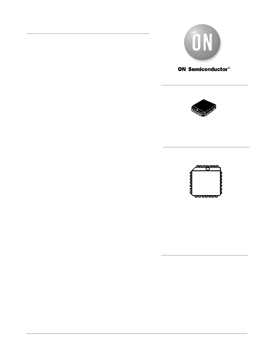
MARKING DIAGRAM*
xxx
= 10 or 100
A
= Assembly Location
WL
= Wafer Lot
YY
= Year
WW
= Work Week
G
= PbFree Package
PLCC28
FN SUFFIX
CASE 776
MCxxxE143FNG
AWLYYWW
1
http://onsemi.com
*For additional marking information, refer to
Application Note AND8002/D.
See detailed ordering and shipping information in the package
dimensions section on page 6 of this data sheet.
ORDERING INFORMATION
相關(guān)PDF資料 |
PDF描述 |
|---|---|
| 5535655-1 | CONN HEADER 68POS MEM CARD T/H |
| 5953398-1 | CONN SMART CARD READER 8POS T/H |
| VE-B3F-MU-B1 | CONVERTER MOD DC/DC 72V 200W |
| VE-B3D-MU-B1 | CONVERTER MOD DC/DC 85V 200W |
| MC10E141FN | IC SHIFT REGISTR 8BIT ECL 28PLCC |
相關(guān)代理商/技術(shù)參數(shù) |
參數(shù)描述 |
|---|---|
| MC10E143FNG | 功能描述:寄存器 5V ECL 9-Bit Hold RoHS:否 制造商:NXP Semiconductors 邏輯類型:CMOS 邏輯系列:HC 電路數(shù)量:1 最大時鐘頻率:36 MHz 傳播延遲時間: 高電平輸出電流:- 7.8 mA 低電平輸出電流:7.8 mA 電源電壓-最大:6 V 最大工作溫度:+ 125 C 封裝 / 箱體:SOT-38 封裝:Tube |
| MC10E143FNR2 | 功能描述:寄存器 5V ECL 9-Bit Hold RoHS:否 制造商:NXP Semiconductors 邏輯類型:CMOS 邏輯系列:HC 電路數(shù)量:1 最大時鐘頻率:36 MHz 傳播延遲時間: 高電平輸出電流:- 7.8 mA 低電平輸出電流:7.8 mA 電源電壓-最大:6 V 最大工作溫度:+ 125 C 封裝 / 箱體:SOT-38 封裝:Tube |
| MC10E143FNR2G | 功能描述:寄存器 5V ECL 9-Bit Hold RoHS:否 制造商:NXP Semiconductors 邏輯類型:CMOS 邏輯系列:HC 電路數(shù)量:1 最大時鐘頻率:36 MHz 傳播延遲時間: 高電平輸出電流:- 7.8 mA 低電平輸出電流:7.8 mA 電源電壓-最大:6 V 最大工作溫度:+ 125 C 封裝 / 箱體:SOT-38 封裝:Tube |
| MC10E150FN | 功能描述:閉鎖 5V ECL 6-bit D-Type RoHS:否 制造商:Micrel 電路數(shù)量:1 邏輯類型:CMOS 邏輯系列:TTL 極性:Non-Inverting 輸出線路數(shù)量:9 高電平輸出電流: 低電平輸出電流: 傳播延遲時間: 電源電壓-最大:12 V 電源電壓-最小:5 V 最大工作溫度:+ 85 C 最小工作溫度:- 40 C 封裝 / 箱體:SOIC-16 封裝:Reel |
| MC10E150FNG | 功能描述:閉鎖 5V ECL 6-bit D-Type RoHS:否 制造商:Micrel 電路數(shù)量:1 邏輯類型:CMOS 邏輯系列:TTL 極性:Non-Inverting 輸出線路數(shù)量:9 高電平輸出電流: 低電平輸出電流: 傳播延遲時間: 電源電壓-最大:12 V 電源電壓-最小:5 V 最大工作溫度:+ 85 C 最小工作溫度:- 40 C 封裝 / 箱體:SOIC-16 封裝:Reel |
發(fā)布緊急采購,3分鐘左右您將得到回復(fù)。