- 您現(xiàn)在的位置:買賣IC網(wǎng) > PDF目錄26791 > MC100E212FN (ON SEMICONDUCTOR) 100E SERIES, POSITIVE EDGE TRIGGERED D FLIP-FLOP, COMPLEMENTARY OUTPUT, PQCC28 PDF資料下載
參數(shù)資料
| 型號: | MC100E212FN |
| 廠商: | ON SEMICONDUCTOR |
| 元件分類: | 鎖存器 |
| 英文描述: | 100E SERIES, POSITIVE EDGE TRIGGERED D FLIP-FLOP, COMPLEMENTARY OUTPUT, PQCC28 |
| 封裝: | PLASTIC, LCC-28 |
| 文件頁數(shù): | 4/7頁 |
| 文件大?。?/td> | 183K |
| 代理商: | MC100E212FN |
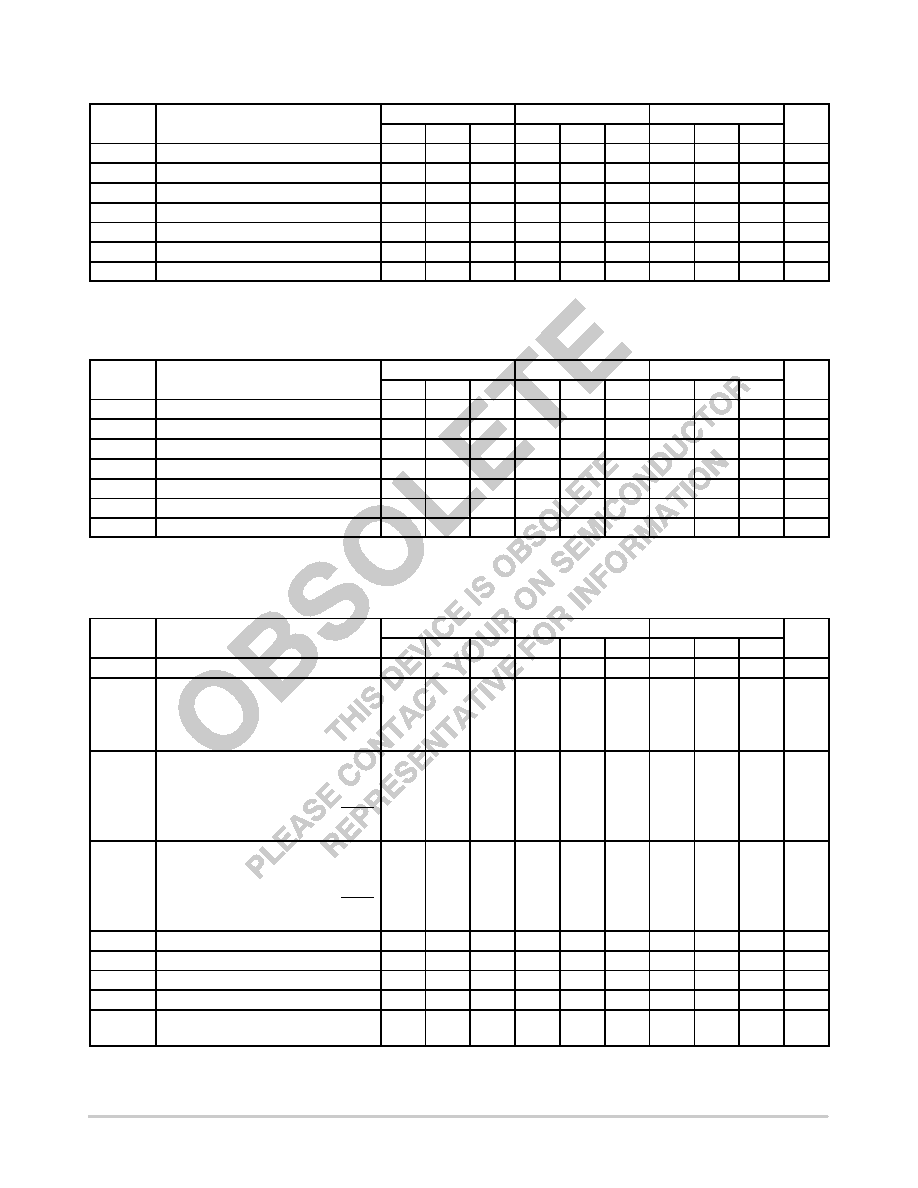
MC10E212, MC100E212
http://onsemi.com
4
0°C
25°C
85°C
Symbol
Characteristic
Min
Typ
Max
Min
Typ
Max
Min
Typ
Max
Unit
IEE
Power Supply Current
80
96
80
96
92
110
mA
VOH
Output HIGH Voltage (Note 2)
3975
4050
4120
3975
4050
4120
3975
4050
4120
mV
VOL
Output LOW Voltage (Note 2)
3190
3295
3380
3190
3255
3380
3190
3260
3380
mV
VIH
Input HIGH Voltage
3835
4050
4120
3835
4120
3835
4120
mV
VIL
Input LOW Voltage
3190
3300
3525
3190
3525
3190
3525
mV
IIH
Input HIGH Current
150
μA
IIL
Input LOW Current
0.5
0.3
0.5
0.25
0.5
0.2
μA
NOTE: Devices are designed to meet the DC specifications shown in the above table, after thermal equilibrium has been established. The
circuit is in a test socket or mounted on a printed circuit board and transverse air flow greater than 500 lfpm is maintained.
1. Input and output parameters vary 1:1 with VCC. VEE can vary +0.4 6V / 0.8 V.
2. Outputs are terminated through a 50 ohm resistor to VCC2 volts.
0°C
25°C
85°C
Symbol
Characteristic
Min
Typ
Max
Min
Typ
Max
Min
Typ
Max
Unit
IEE
Power Supply Current
80
96
80
96
92
110
mA
VOH
Output HIGH Voltage (Note 2)
1025
950
880
1025
950
880
1025
950
880
mV
VOL
Output LOW Voltage (Note 2)
1810 1705 1620 1810 1745 1620 1810 1740 1620
mV
VIH
Input HIGH Voltage
1165
950
880
1165
880
1165
880
mV
VIL
Input LOW Voltage
1810 1700 1475 1810 1475 1475 1810 1475 1475
mV
IIH
Input HIGH Current
150
μA
IIL
Input LOW Current
0.5
0.3
0.5
0.25
0.5
0.2
μA
NOTE: Devices are designed to meet the DC specifications shown in the above table, after thermal equilibrium has been established. The
circuit is in a test socket or mounted on a printed circuit board and transverse air flow greater than 500 lfpm is maintained.
1. Input and output parameters vary 1:1 with VCC. VEE can vary +0.46 V / 0.8 V.
2. Outputs are terminated through a 50 ohm resistor to VCC2 volts.
0°C
25°C
85°C
Symbol
Characteristic
Min
Typ
Max
Min
Typ
Max
Min
Typ
Max
Unit
fMAX
Maximum Toggle Frequency
TBD
GHz
tPLH
Propagation Delay to Output
ps
tPHL
CLK
575
800
1025
575
800
1025
575
800
1025
MR
575
800
1025
575
800
1025
575
800
1025
CLK to S-OUT
575
800
1025
575
800
1025
575
800
1025
ts
Setup Time
ps
D
175
25
175
25
175
25
SHIFT
150
50
150
50
150
50
LOAD
225
50
225
50
225
50
S-IN
150
50
150
50
150
50
th
Hold Time
ps
D
250
25
250
25
250
25
SHIFT
300
100
300
100
300
100
LOAD
225
0
225
0
225
0
S-IN
300
100
300
100
300
100
tRR
Reset Recovery
600
350
600
350
600
350
ps
tSKEW
Within-Device Skew (Note 1.)
100
ps
tSKEW
Within-Gate Skew (Note 2.)
50
ps
tJITTER
CycletoCycle Jitter
TBD
ps
tr
Rise/Fall Times
ps
tf
(20 - 80%)
275
425
650
275
425
650
275
425
650
1. 10 Series: VEE can vary +0.46 V / 0.06 V.
100 Series: VEE can vary +0.46 V / 0.8 V.
1. Within-device skew is defined as identical transitions on similar paths through a device.
相關(guān)PDF資料 |
PDF描述 |
|---|---|
| MC100E256FN | 100E SERIES, LOW LEVEL TRIGGERED D LATCH, COMPLEMENTARY OUTPUT, PQCC28 |
| MC100E452FNR2 | 100E SERIES, D FLIP-FLOP, PQCC28 |
| MC100EL04DR2 | 100EL SERIES, 2-INPUT AND/NAND GATE, PDSO8 |
| MC100EL14DWR2 | 100EL SERIES, LOW SKEW CLOCK DRIVER, 5 TRUE OUTPUT(S), 0 INVERTED OUTPUT(S), PDSO20 |
| MC100EL35D | 100EL SERIES, POSITIVE EDGE TRIGGERED J-K FLIP-FLOP, COMPLEMENTARY OUTPUT, PDSO8 |
相關(guān)代理商/技術(shù)參數(shù) |
參數(shù)描述 |
|---|---|
| MC100E212FNR2 | 制造商:ONSEMI 制造商全稱:ON Semiconductor 功能描述:5V ECL 3-Bit Scannable Registered Address Driver |
| MC100E241 | 制造商:ONSEMI 制造商全稱:ON Semiconductor 功能描述:8-BIT SCANNABLE REGISTER |
| MC100E241_06 | 制造商:ONSEMI 制造商全稱:ON Semiconductor 功能描述:5V ECL 8-Bit Scannable Register |
| MC100E241FN | 功能描述:寄存器 5V ECL 8-Bit RoHS:否 制造商:NXP Semiconductors 邏輯類型:CMOS 邏輯系列:HC 電路數(shù)量:1 最大時鐘頻率:36 MHz 傳播延遲時間: 高電平輸出電流:- 7.8 mA 低電平輸出電流:7.8 mA 電源電壓-最大:6 V 最大工作溫度:+ 125 C 封裝 / 箱體:SOT-38 封裝:Tube |
| MC100E241FNG | 功能描述:寄存器 5V ECL 8-Bit Scannable RoHS:否 制造商:NXP Semiconductors 邏輯類型:CMOS 邏輯系列:HC 電路數(shù)量:1 最大時鐘頻率:36 MHz 傳播延遲時間: 高電平輸出電流:- 7.8 mA 低電平輸出電流:7.8 mA 電源電壓-最大:6 V 最大工作溫度:+ 125 C 封裝 / 箱體:SOT-38 封裝:Tube |
發(fā)布緊急采購,3分鐘左右您將得到回復(fù)。