- 您現(xiàn)在的位置:買賣IC網(wǎng) > PDF目錄45201 > MB9AF114LPMC RISC MICROCONTROLLER, PQFP64 PDF資料下載
參數(shù)資料
| 型號: | MB9AF114LPMC |
| 元件分類: | 微控制器/微處理器 |
| 英文描述: | RISC MICROCONTROLLER, PQFP64 |
| 封裝: | 0.65 MM PITCH, PLASTIC, LQFP-64 |
| 文件頁數(shù): | 73/112頁 |
| 文件大小: | 1225K |
| 代理商: | MB9AF114LPMC |
第1頁第2頁第3頁第4頁第5頁第6頁第7頁第8頁第9頁第10頁第11頁第12頁第13頁第14頁第15頁第16頁第17頁第18頁第19頁第20頁第21頁第22頁第23頁第24頁第25頁第26頁第27頁第28頁第29頁第30頁第31頁第32頁第33頁第34頁第35頁第36頁第37頁第38頁第39頁第40頁第41頁第42頁第43頁第44頁第45頁第46頁第47頁第48頁第49頁第50頁第51頁第52頁第53頁第54頁第55頁第56頁第57頁第58頁第59頁第60頁第61頁第62頁第63頁第64頁第65頁第66頁第67頁第68頁第69頁第70頁第71頁第72頁當前第73頁第74頁第75頁第76頁第77頁第78頁第79頁第80頁第81頁第82頁第83頁第84頁第85頁第86頁第87頁第88頁第89頁第90頁第91頁第92頁第93頁第94頁第95頁第96頁第97頁第98頁第99頁第100頁第101頁第102頁第103頁第104頁第105頁第106頁第107頁第108頁第109頁第110頁第111頁第112頁
63
FUJITSU SEMICONDUCTOR CONFIDENTIAL
r2.1
MB9A110 Series
DS706-00011-1v0-E
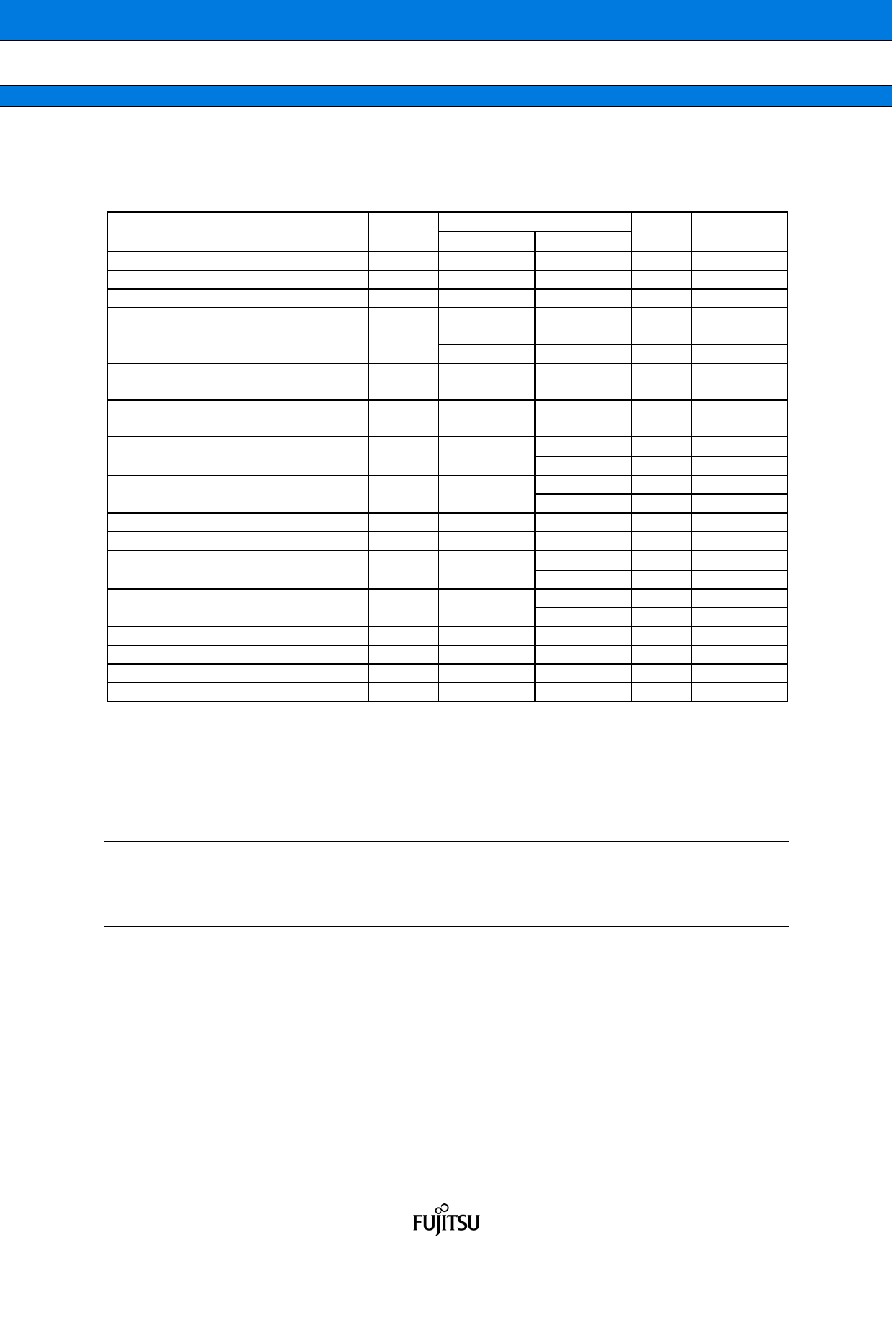
ELECTRICAL CHARACTERISTICS
1. Absolute Maximum Ratings
Rating
Parameter
Symbol
Min
Max
Unit
Remarks
Power supply voltage*1, *2
Vcc
Vss - 0.5
Vss + 6.5
V
Analog power supply voltage*1, *3
AVcc
Vss - 0.5
Vss + 6.5
V
Analog reference voltage*1, *3
AVRH
Vss - 0.5
Vss + 6.5
V
Vss - 0.5
Vcc + 0.5
(≤ 6.5V)
V
Input voltage*1
VI
Vss - 0.5
Vss + 6.5
V
5V tolerant
Analog pin input voltage*1
VIA
Vss - 0.5
AVcc + 0.5
(≤ 6.5V)
V
Output voltage*1
VO
Vss - 0.5
Vcc + 0.5
(≤ 6.5V)
V
10
mA
4mA type
"L" level maximum output current*4
IOL
-
20
mA
12mA type
4
mA
4mA type
"L" level average output current*5
IOLAV
-
12
mA
12mA type
"L" level total maximum output current
∑IOL
-
100
mA
"L" level total average output current*6
∑IOLAV
-
50
mA
- 10
mA
4mA type
"H" level maximum output current*4
IOH
-
- 20
mA
12mA type
- 4
mA
4mA type
"H" level average output current*5
IOHAV
-
- 12
mA
12mA type
"H" level total maximum output current
∑IOH
-
- 100
mA
"H" level total average output current*6
∑IOHAV
-
- 50
mA
Power consumption
PD
-
300
mW
Storage temperature
TSTG
- 55
+ 150
°C
*1 : These parameters are based on the condition that Vss = AVss = 0.0V.
*2 : Vcc must not drop below Vss - 0.5V.
*3 : Be careful not to exceed Vcc + 0.5 V, for example, when the power is turned on.
*4 : The maximum output current is the peak value for a single pin.
*5 : The average output is the average current for a single pin over a period of 100 ms.
*6 : The total average output current is the average current for all pins over a period of 100 ms.
<WARNING>
Semiconductor devices can be permanently damaged by application of stress (voltage, current, temperature,
etc.) in excess of absolute maximum ratings. Do not exceed these ratings.
相關(guān)PDF資料 |
PDF描述 |
|---|---|
| MB9AF112MPMC | RISC MICROCONTROLLER, PQFP80 |
| MB9AF112LPMC1 | RISC MICROCONTROLLER, PQFP64 |
| MB9AF112NPMC | RISC MICROCONTROLLER, PQFP100 |
| MB9AF111NPF | RISC MICROCONTROLLER, PQFP100 |
| MB9AF311NPF | 32-BIT, FLASH, 40 MHz, RISC MICROCONTROLLER, PQFP100 |
相關(guān)代理商/技術(shù)參數(shù) |
參數(shù)描述 |
|---|---|
| MB9AF114LPMC1-GE1 | 制造商:FUJITSU 功能描述: |
| MB9AF114LPMC1-G-JNE1 | 制造商:FUJITSU 功能描述: 制造商:FUJITSU 功能描述:MCU 32BIT CORTEX-M3 FM3 64LQFP |
| MB9AF114MAPMC-G-JNE2 | 制造商:Fujitsu 功能描述:Bulk |
| MB9AF114MPMC-G-JNE1 | 制造商:FUJITSU 功能描述:MCU 32BIT CORTEX-M3 FM3 80LQFP |
| MB9AF114NAPMC-G-JNE2 | 制造商:FUJITSU 功能描述: 制造商:Fujitsu 功能描述:Bulk |
發(fā)布緊急采購,3分鐘左右您將得到回復(fù)。