- 您現(xiàn)在的位置:買賣IC網(wǎng) > PDF目錄45201 > MB9AF112NPF (FUJITSU LTD) 32-BIT, FLASH, RISC MICROCONTROLLER, PQFP100 PDF資料下載
參數(shù)資料
| 型號: | MB9AF112NPF |
| 廠商: | FUJITSU LTD |
| 元件分類: | 微控制器/微處理器 |
| 英文描述: | 32-BIT, FLASH, RISC MICROCONTROLLER, PQFP100 |
| 封裝: | 14 X 20 MM, 3.35 MM HEIGHT, 0.65 MM PITCH, PLASTIC, LQFP-100 |
| 文件頁數(shù): | 55/108頁 |
| 文件大?。?/td> | 1221K |
| 代理商: | MB9AF112NPF |
第1頁第2頁第3頁第4頁第5頁第6頁第7頁第8頁第9頁第10頁第11頁第12頁第13頁第14頁第15頁第16頁第17頁第18頁第19頁第20頁第21頁第22頁第23頁第24頁第25頁第26頁第27頁第28頁第29頁第30頁第31頁第32頁第33頁第34頁第35頁第36頁第37頁第38頁第39頁第40頁第41頁第42頁第43頁第44頁第45頁第46頁第47頁第48頁第49頁第50頁第51頁第52頁第53頁第54頁當前第55頁第56頁第57頁第58頁第59頁第60頁第61頁第62頁第63頁第64頁第65頁第66頁第67頁第68頁第69頁第70頁第71頁第72頁第73頁第74頁第75頁第76頁第77頁第78頁第79頁第80頁第81頁第82頁第83頁第84頁第85頁第86頁第87頁第88頁第89頁第90頁第91頁第92頁第93頁第94頁第95頁第96頁第97頁第98頁第99頁第100頁第101頁第102頁第103頁第104頁第105頁第106頁第107頁第108頁
50
MB9A110 Series
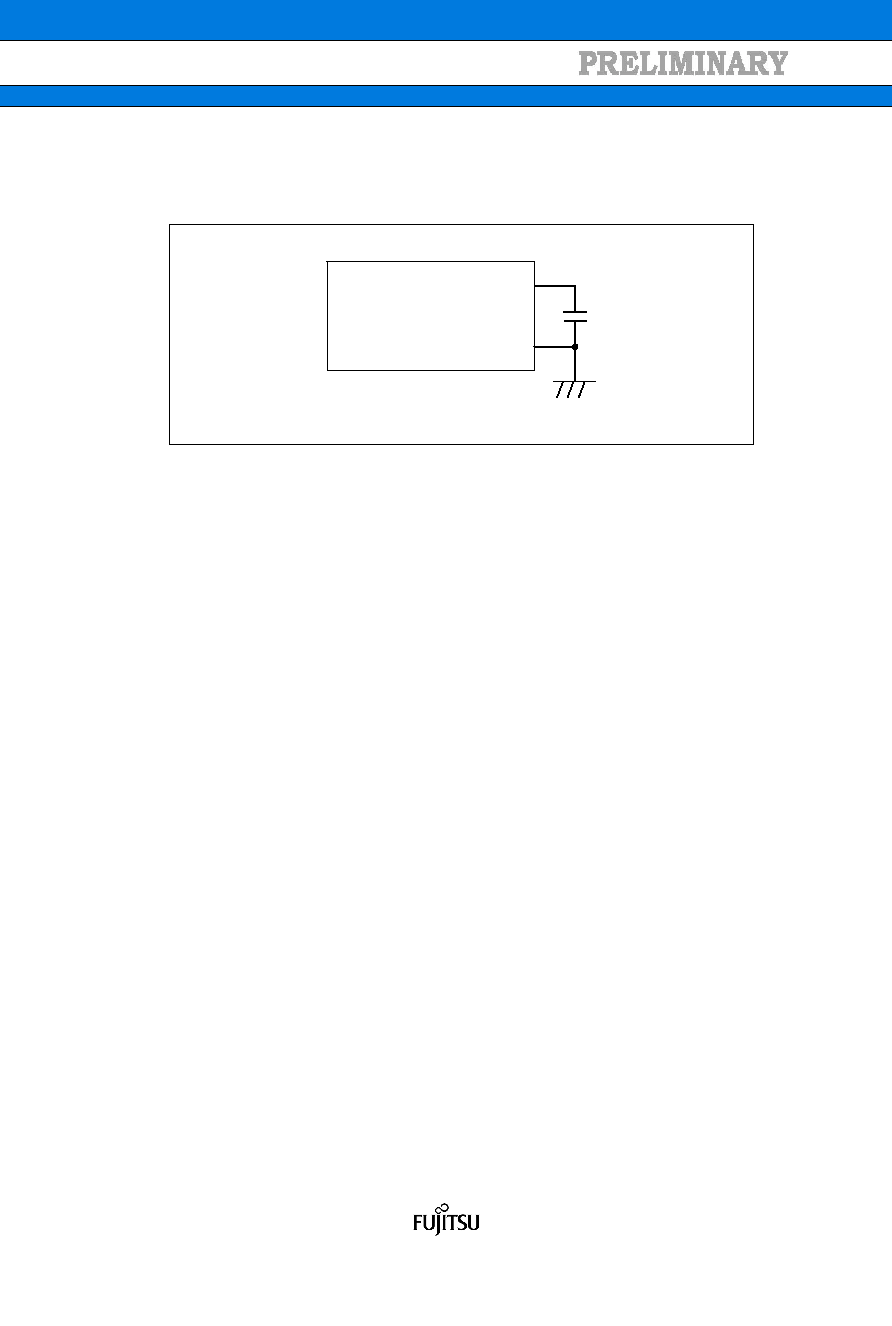
C Pin
As this series includes an internal regulator, always connect a bypass capacitor of approximately 4.7 F to
the C pin for use by the regulator.
GND
4.7μF
VSS
C
Device
Mode pins (MD0)
Connect the MD pin (MD0) directly to VCC or VSS pins. Design the printed circuit board such that the
pull-up/down resistance stays low, as well as the distance between the mode pins and VCC pins or VSS pins
is as short as possible and the connection impedance is low, when the pins are pulled-up/down such as for
switching the pin level and rewriting the Flash memory data. It is because of preventing the device
erroneously switching to test mode due to noise.
Notes on power-on
Turn power on/off in the following order or at the same time.
If not using the A/D converter, connect AVCC =VCC and AVSS = VSS.
Turning on : VCC
AVCC AVRH
Turning off : AVRH
AVCC VCC
Serial Communication
There is a possibility to receive wrong data due to the noise or other causes on the serial communication.
Therefore, design a printed circuit board so as to avoid noise.
Consider the case of receiving wrong data due to noise, perform error detection such as by applying a
checksum of data at the end. If an error is detected, restransmit the data.
Differences in features among the products with different memory sizes and
between FLASH products and MASK products
The electric characteristics including power consumption, ESD, latch-up, noise characteristics, and
oscillation characteristics among the products with different memory sizes and between FLASH products
and MASK products are different because chip layout and memory structures are different.
If you are switching to use a different product of the same series, please make sure to evaluate the electric
characteristics.
FUJITSU SEMICONDUCTOR CONFIDENTIAL
r1.0
DS706-00011-0v01-E
相關PDF資料 |
PDF描述 |
|---|---|
| MB9AF112NBGL | 32-BIT, FLASH, RISC MICROCONTROLLER, PBGA112 |
| MB9AF116NPF | 32-BIT, FLASH, RISC MICROCONTROLLER, PQFP100 |
| MB9AF112NPMC | 32-BIT, FLASH, RISC MICROCONTROLLER, PQFP100 |
| MB9AF114LPMC | 32-BIT, FLASH, RISC MICROCONTROLLER, PQFP64 |
| MB9AF112LPMC1 | 32-BIT, FLASH, RISC MICROCONTROLLER, PQFP64 |
相關代理商/技術(shù)參數(shù) |
參數(shù)描述 |
|---|---|
| MB9AF114LAPMC1-G-JNE2 | 制造商:Fujitsu 功能描述:Bulk |
| MB9AF114LPMC1-GE1 | 制造商:FUJITSU 功能描述: |
| MB9AF114LPMC1-G-JNE1 | 制造商:FUJITSU 功能描述: 制造商:FUJITSU 功能描述:MCU 32BIT CORTEX-M3 FM3 64LQFP |
| MB9AF114MAPMC-G-JNE2 | 制造商:Fujitsu 功能描述:Bulk |
| MB9AF114MPMC-G-JNE1 | 制造商:FUJITSU 功能描述:MCU 32BIT CORTEX-M3 FM3 80LQFP |
發(fā)布緊急采購,3分鐘左右您將得到回復。