- 您現(xiàn)在的位置:買(mǎi)賣(mài)IC網(wǎng) > PDF目錄98011 > MB96F315RSAPMC-GSE2 (FUJITSU LTD) RISC MICROCONTROLLER, PQFP48 PDF資料下載
參數(shù)資料
| 型號(hào): | MB96F315RSAPMC-GSE2 |
| 廠商: | FUJITSU LTD |
| 元件分類(lèi): | 微控制器/微處理器 |
| 英文描述: | RISC MICROCONTROLLER, PQFP48 |
| 封裝: | 7 X 7 MM, 1.70 MM HEIGHT, 0.50 MM PITCH, PLASTIC, LQFP-48 |
| 文件頁(yè)數(shù): | 42/74頁(yè) |
| 文件大?。?/td> | 2025K |
| 代理商: | MB96F315RSAPMC-GSE2 |
第1頁(yè)第2頁(yè)第3頁(yè)第4頁(yè)第5頁(yè)第6頁(yè)第7頁(yè)第8頁(yè)第9頁(yè)第10頁(yè)第11頁(yè)第12頁(yè)第13頁(yè)第14頁(yè)第15頁(yè)第16頁(yè)第17頁(yè)第18頁(yè)第19頁(yè)第20頁(yè)第21頁(yè)第22頁(yè)第23頁(yè)第24頁(yè)第25頁(yè)第26頁(yè)第27頁(yè)第28頁(yè)第29頁(yè)第30頁(yè)第31頁(yè)第32頁(yè)第33頁(yè)第34頁(yè)第35頁(yè)第36頁(yè)第37頁(yè)第38頁(yè)第39頁(yè)第40頁(yè)第41頁(yè)當(dāng)前第42頁(yè)第43頁(yè)第44頁(yè)第45頁(yè)第46頁(yè)第47頁(yè)第48頁(yè)第49頁(yè)第50頁(yè)第51頁(yè)第52頁(yè)第53頁(yè)第54頁(yè)第55頁(yè)第56頁(yè)第57頁(yè)第58頁(yè)第59頁(yè)第60頁(yè)第61頁(yè)第62頁(yè)第63頁(yè)第64頁(yè)第65頁(yè)第66頁(yè)第67頁(yè)第68頁(yè)第69頁(yè)第70頁(yè)第71頁(yè)第72頁(yè)第73頁(yè)第74頁(yè)

PRELIMINARY
MB96310 Series
FME-MB96310 rev 2
47
*2: VI and VO should not exceed VCC + 0.3 V. VI should also not exceed the specied ratings. However if the
maximum current to/from a input is limited by some means with external components, the ICLAMP rating super-
sedes the VI rating. Input/output voltages of standard ports depend on VCC.
*3:
Applicable to all general purpose I/O pins (Pnn_m)
Use within recommended operating conditions.
Use at DC voltage (current)
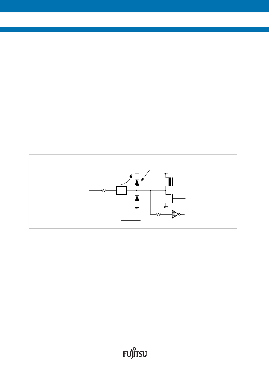
The +B signal should always be applied a limiting resistance placed between the +B signal and the
microcontroller.
The value of the limiting resistance should be set so that when the +B signal is applied the input current to
the microcontroller pin does not exceed rated values, either instantaneously or for prolonged periods.
Note that when the microcontroller drive current is low, such as in the power saving modes, the +B input
potential may pass through the protective diode and increase the potential at the VCC pin, and this may affect
other devices.
Note that if a +B signal is input when the microcontroller power supply is off (not xed at 0 V), the power
supply is provided from the pins, so that incomplete operation may result.
Note that if the +B input is applied during power-on, the power supply is provided from the pins and the resulting
supply voltage may not be sufcient to operate the Power reset (except devices with persistent low voltage
reset in internal vector mode).
Sample recommended circuits:
*4: The maximum permitted power dissipation depends on the ambient temperature, the air ow velocity and the
thermal conductance of the package on the PCB.
The actual power dissipation depends on the customer application and can be calculated as follows:
PD = PIO + PINT
PIO =
∑ (VOL * IOL + VOH * IOH) (IO load power dissipation, sum is performed on all IO ports)
PINT = VCC * (ICC + IA) (internal power dissipation)
ICC is the total core current consumption into VCC as described in the “DC characteristics” and depends on the
selected operation mode and clock frequency and the usage of functions like Flash programming or the clock
modulator.
IA is the analog current consumption into AVCC.
*5: Worst case value for a package mounted on single layer PCB at specied TA without air ow.
*6: Please contact Fujitsu for reliability limitations when using under these conditions.
WARNING: Semiconductor devices can be permanently damaged by application of stress (voltage, current,
temperature, etc.) in excess of absolute maximum ratings. Do not exceed these ratings.
P-ch
N-ch
VCC
R
Protective Diode
Limiting
resistance
+B input (0V to 16V)
相關(guān)PDF資料 |
PDF描述 |
|---|---|
| MB96F315RWAPMC-GSE2 | RISC MICROCONTROLLER, PQFP48 |
| MB96F315YWAPMC-GSE2 | RISC MICROCONTROLLER, PQFP48 |
| MB96F313YWAPMC-GSE2 | RISC MICROCONTROLLER, PQFP48 |
| MB96F348RSBPQC-GSE2 | 16-BIT, FLASH, 56 MHz, MICROCONTROLLER, PQFP100 |
| MB9BF504NAPMC | 32-BIT, FLASH, 80 MHz, RISC MICROCONTROLLER, PQFP100 |
相關(guān)代理商/技術(shù)參數(shù) |
參數(shù)描述 |
|---|---|
| MB96F315RSBPMC-GSE1 | 制造商:FUJITSU 制造商全稱(chēng):Fujitsu Component Limited. 功能描述:16-bit Proprietary Microcontroller |
| MB96F315RSBPMC-GSE2 | 制造商:FUJITSU 功能描述: 制造商:FUJITSU 功能描述:MCU 16BIT 16FX 160K FLASH 48LQFP 制造商:FUJITSU 功能描述:MCU, 16BIT, 16FX, 160K FLASH, 48LQFP 制造商:FUJITSU 功能描述:MCU, 16BIT, 16FX, 160K FLASH, 48LQFP, Controller Family/Series:MB96310, Core Size:16bit, No. of I/O's:36, Supply Voltage Min:3V, Supply Voltage Max:5.5V, Digital IC Case Style:LQFP, No. of Pins:48, Program Memory Size:160KB, RAM |
| MB96F315RWAPMC-ESE2 | 制造商:FUJITSU 功能描述: |
| MB96F315RWBPMC-ESE2 | 制造商:FUJITSU 功能描述: |
| MB96F315RWBPMC-GSE2 | 制造商:FUJITSU 制造商全稱(chēng):Fujitsu Component Limited. 功能描述:16-bit Proprietary Microcontroller |
發(fā)布緊急采購(gòu),3分鐘左右您將得到回復(fù)。