- 您現(xiàn)在的位置:買賣IC網(wǎng) > PDF目錄16169 > MAX9218EVKIT+ (Maxim Integrated Products)KIT PCB EVALUATION FOR MAX9218 PDF資料下載
參數(shù)資料
| 型號(hào): | MAX9218EVKIT+ |
| 廠商: | Maxim Integrated Products |
| 文件頁(yè)數(shù): | 4/15頁(yè) |
| 文件大?。?/td> | 0K |
| 描述: | KIT PCB EVALUATION FOR MAX9218 |
| 產(chǎn)品培訓(xùn)模塊: | Lead (SnPb) Finish for COTS Obsolescence Mitigation Program |
| 標(biāo)準(zhǔn)包裝: | 1 |
| 系列: | * |
第1頁(yè)第2頁(yè)第3頁(yè)當(dāng)前第4頁(yè)第5頁(yè)第6頁(yè)第7頁(yè)第8頁(yè)第9頁(yè)第10頁(yè)第11頁(yè)第12頁(yè)第13頁(yè)第14頁(yè)第15頁(yè)
MAX9218
27-Bit, 3MHz-to-35MHz
DC-Balanced LVDS Deserializer
12
______________________________________________________________________________________
Input Frequency Detection
A frequency-detection circuit detects when the LVDS
input is not switching. When not switching, all outputs
except LOCK are low, LOCK is high, and PCLK_OUT
follows REFCLK. This condition occurs, for example, if
the serializer is not driving the interconnect or if the
interconnect is open.
Frequency Range Setting (RNG[1:0])
The RNG[1:0] inputs select the operating frequency
range of the MAX9218 and the transition time of the out-
puts. Select the frequency range that includes the
MAX9217 serializer PCLK_IN frequency. Table 3 shows
the selectable frequency ranges and the corresponding
data rates and output transition times.
Power Down
Driving PWRDWN low puts the outputs in high imped-
ance and stops the PLL. With PWRDWN
≤ 0.3V and all
LVTTL/LVCMOS inputs
≤ 0.3V or ≥ VCC - 0.3V, the sup-
ply current is reduced to less than 50A. Driving
PWRDWN high initiates lock to the local reference clock
(REFCLK) and afterwards to the serial input.
Lock and Loss of Lock (LOCK)
When PWRDWN is driven high, the PLL begins locking
to REFCLK, drives LOCK from high impedance to high
and the other outputs from high impedance to low
except PCLK_OUT. PCLK_OUT outputs REFCLK while
the PLL is locking to REFCLK. Locking to REFCLK
takes a maximum of 16,385 REFCLK cycles. When
locking to REFCLK is complete, the serial input is moni-
tored for a transition word. When a transition word is
found, LOCK is driven low indicating valid output data,
and the parallel rate clock recovered from the serial
input is output on PCLK_OUT. PCLK_OUT is stretched
on the change from REFCLK to recovered clock (or
vice versa).
If a transition word is not detected within 220 cycles of
PCLK_OUT, LOCK is driven high and the other outputs
except PCLK_OUT are driven low. REFCLK is output on
PCLK_OUT and the deserializer continues monitoring
the serial input for a transition word. See Figure 7 for
the synchronization timing diagram.
Output Enable (OUTEN) and
Busing Outputs
The outputs of two MAX9218s can be bused to form a
2:1 mux with the outputs controlled by the output
enable. Wait 30ns between disabling one deserializer
(driving OUTEN low) and enabling the second one (dri-
ving OUTEN high) to avoid contention of the bused out-
puts. OUTEN controls all outputs.
Rising or Falling Output Latch Edge (R/F)
The MAX9218 has a selectable rising or falling output
latch edge through a logic setting on R/F. Driving R/F
high selects the rising output latch edge, which latches
the parallel output data into the next chip on the rising
edge of PCLK_OUT. Driving R/F low selects the falling
output latch edge, which latches the parallel output
data into the next chip on the falling edge of
PCLK_OUT. The MAX9218 output-latch-edge polarity
does not need to match the MAX9217 serializer input-
latch-edge polarity. Select the latch-edge polarity
required by the chip being driven by the MAX9218.
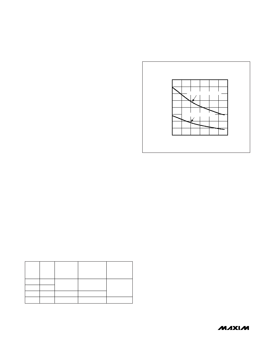
AC-COUPLING CAPACITOR VALUE
vs. PARALLEL CLOCK FREQUENCY
PARALLEL CLOCK FREQUENCY (MHz)
CAPACITOR
VALUE
(nF)
33
30
21
24
27
35
50
65
80
95
110
125
140
20
18
36
TWO CAPACITORS PER LINK
FOUR CAPACITORS PER LINK
RNG1
RNG0
PARALLEL
CLOCK
(MHz)
SERIAL
DATA RATE
(Mbps)
OUTPUT
TRANSITION
TIME
00
01
3 to 7
60 to 140
1
0
7 to 15
140 to 300
Slow
1
15 to 35
300 to 700
Fast
Figure 12. AC-Coupling Capacitor Values vs. Clock Frequency
of 18MHz to 35MHz
Table 3. Frequency Range Programming
相關(guān)PDF資料 |
PDF描述 |
|---|---|
| VE-24R-EY-S | CONVERTER MOD DC/DC 7.5V 50W |
| VE-24P-EY-S | CONVERTER MOD DC/DC 13.8V 50W |
| MAX9217EVKIT+ | KIT PCB EVALUATION FOR MAX9217 |
| MAX5393EVKIT+ | KIT EVALUATION FOR MAX5393 |
| 383LX124M016N082 | CAP ALUM 120000UF 16V 20% SNAP |
相關(guān)代理商/技術(shù)參數(shù) |
參數(shù)描述 |
|---|---|
| MAX9218EVKIT+ | 功能描述:界面開(kāi)發(fā)工具 MAX9217/18 Eval Kit RoHS:否 制造商:Bourns 產(chǎn)品:Evaluation Boards 類型:RS-485 工具用于評(píng)估:ADM3485E 接口類型:RS-485 工作電源電壓:3.3 V |
| MAX921C/D | 功能描述:校驗(yàn)器 IC RoHS:否 制造商:STMicroelectronics 產(chǎn)品: 比較器類型: 通道數(shù)量: 輸出類型:Push-Pull 電源電壓-最大:5.5 V 電源電壓-最小:1.1 V 補(bǔ)償電壓(最大值):6 mV 電源電流(最大值):1350 nA 響應(yīng)時(shí)間: 最大工作溫度:+ 125 C 安裝風(fēng)格:SMD/SMT 封裝 / 箱體:SC-70-5 封裝:Reel |
| MAX921C/D DIE | 制造商:Maxim Integrated Products 功能描述: |
| MAX921C/D+ | 功能描述:校驗(yàn)器 IC RoHS:否 制造商:STMicroelectronics 產(chǎn)品: 比較器類型: 通道數(shù)量: 輸出類型:Push-Pull 電源電壓-最大:5.5 V 電源電壓-最小:1.1 V 補(bǔ)償電壓(最大值):6 mV 電源電流(最大值):1350 nA 響應(yīng)時(shí)間: 最大工作溫度:+ 125 C 安裝風(fēng)格:SMD/SMT 封裝 / 箱體:SC-70-5 封裝:Reel |
| MAX921CPA | 功能描述:校驗(yàn)器 IC Single Comparator w/1% Precision Ref RoHS:否 制造商:STMicroelectronics 產(chǎn)品: 比較器類型: 通道數(shù)量: 輸出類型:Push-Pull 電源電壓-最大:5.5 V 電源電壓-最小:1.1 V 補(bǔ)償電壓(最大值):6 mV 電源電流(最大值):1350 nA 響應(yīng)時(shí)間: 最大工作溫度:+ 125 C 安裝風(fēng)格:SMD/SMT 封裝 / 箱體:SC-70-5 封裝:Reel |
發(fā)布緊急采購(gòu),3分鐘左右您將得到回復(fù)。