- 您現(xiàn)在的位置:買賣IC網(wǎng) > PDF目錄385555 > MAX9178EUE (MAXIM INTEGRATED PRODUCTS INC) Quad LVDS Line Driver with High-ESD Tolerance and Flow-Through Pinout PDF資料下載
參數(shù)資料
| 型號: | MAX9178EUE |
| 廠商: | MAXIM INTEGRATED PRODUCTS INC |
| 元件分類: | 通用總線功能 |
| 英文描述: | Quad LVDS Line Driver with High-ESD Tolerance and Flow-Through Pinout |
| 中文描述: | QUAD LINE DRIVER, PDSO16 |
| 封裝: | 4.40 MM, TSSOP-16 |
| 文件頁數(shù): | 3/14頁 |
| 文件大?。?/td> | 319K |
| 代理商: | MAX9178EUE |
M
Quad LVDS Line Driver with High-ESD
Tolerance and Flow-Through Pinout
_______________________________________________________________________________________
3
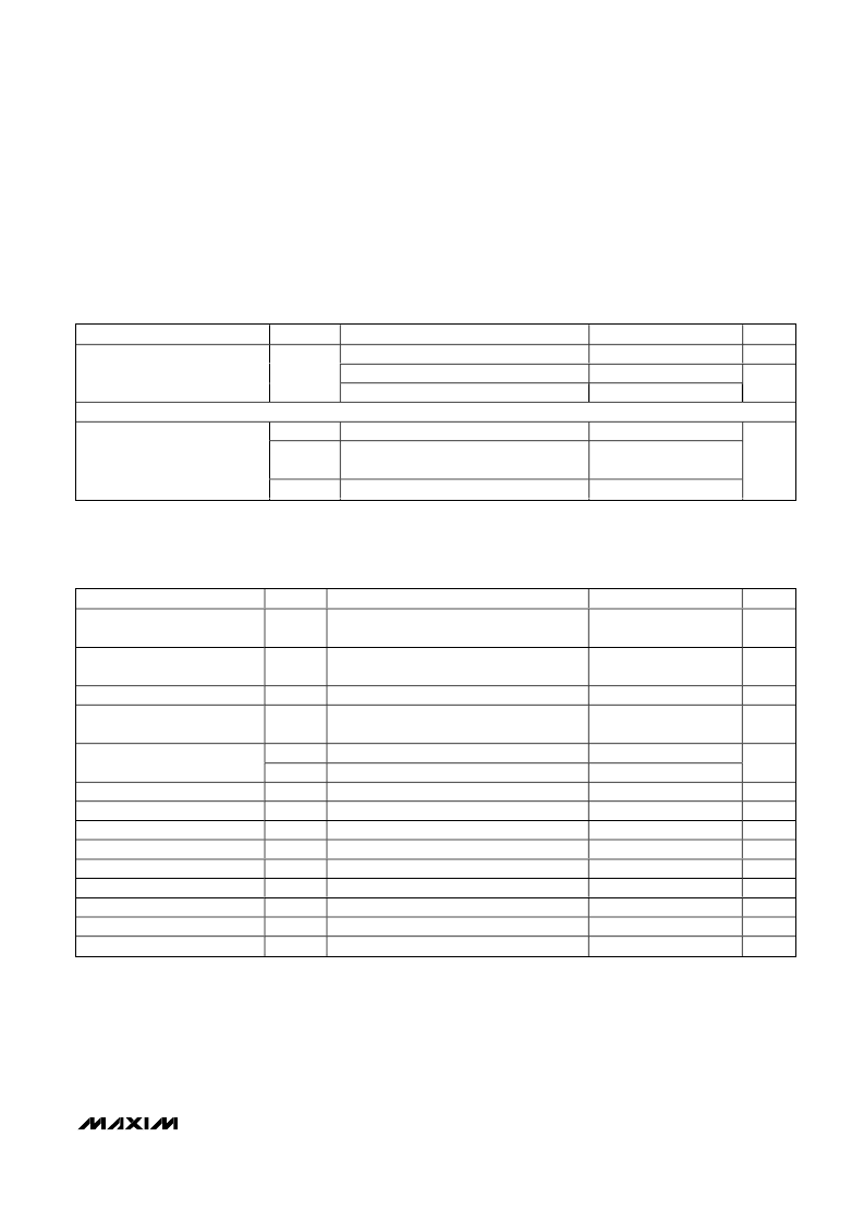
DC ELECTRICAL CHARACTERISTICS (continued)
(V
CC
= +3.0V to +3.6V, R
L
= 100
±1%, IN_ = high or low, EN = high,
EN
= low, T
A
= -40
°
C to +85
°
C. Typical values are at V
CC
=
+3.3V, T
A
= +25
°
C, unless otherwise noted.) (Notes 1, 2)
SWITCHING CHARACTERISTICS
(V
CC
= +3.0V to +3.6V, R
L
= 100
±1%, C
L
= 15pF, T
A
= -40
°
C to +85
°
C. Typical values are at V
CC
= +3.3V, T
A
= +25
°
C, unless
otherwise noted.) (Notes 4
–
7)
Note 1:
Maximum and minimum limits over temperature are guaranteed by design and characterization. Devices are 100% tested
at T
A
= +85
°
C.
Note 2:
Currents into the device are positive, and current out of the device is negative. All voltages are referenced to ground
except V
OD
,
V
OD
, V
OS
, and
V
OS
.
Note 3:
Guaranteed by design.
Note 4:
AC parameters are guaranteed by design and characterization. Limits are set at ±6 sigma.
Note 5:
C
L
includes probe and jig capacitance.
Note 6:
Pulse generator output for AC tests: t
R
= t
F
= 1ns (0.2 x V
CC
to 0.8 x V
CC
), 50% duty cycle, R
O
= 50
, V
OH
= V
CC
+ 1V set-
tling to V
CC
, V
OL
= -1V settling to zero, frequency = 200MHz.
PARAMETER
SYMBOL
CONDITIONS
MIN
-20
TYP
5
0.67
-0.46
MAX
+20
1.5
UNITS
μA
0
≤
IN_, EN,
EN
≤
V
CC
V
CC
≤
IN_, EN,
EN
≤
V
CC
+ 1
-1V
≤
IN_, EN,
EN
≤
0
Input Current
I
IN
-1.5
mA
SUPPLY CURRENT
I
CC
IN_ = V
CC
or 0, EN = V
CC
,
EN
= 0, no load
IN_ = V
CC
or 0, EN = V
CC
,
EN
= 0,
outputs loaded
3.8
6.0
I
CCL
18
25
Supply Current
I
CCZ
IN_ = V
CC
or 0, EN = 0,
EN
= V
CC
3.8
6
mA
PARAMETER
SYMBOL
CONDITIONS
MIN
TYP
MAX
UNITS
Differential Propagation Delay
High to Low
t
PHLD
Figures 2, 3
0.9
1.4
2.0
ns
Differential Propagation Delay
Low to High
t
PLHD
Figures 2, 3
0.9
1.5
2.0
ns
Differential Pulse Skew
t
SKD1
Figures 2, 3 (Note 8)
0.1
0.25
ns
Differential Channel-to-Channel
Skew
t
SKD2
Figures 2, 3 (Note 9)
0.15
0.35
ns
t
SKD3
t
SKD4
t
R
t
F
t
PHZ
t
PLZ
t
PZH
t
PZL
t
AH
t
HA
f
MAX
Figures 2, 3 (Note 10)
Figures 2, 3 (Note 11)
Figures 2, 3
Figures 2, 3
Figures 4, 5
Figures 4, 5
Figures 4, 5
Figures 4, 5
R
L
= 80
to 132
±
1%; Figures 6, 7
R
L
= 80
to 132
±
1%; Figures 6, 7 (Note 12)
(Note 13)
0.9
1.1
0.70
0.70
5
5
7
7
100
1.5
Differential Part-to-Part Skew
ns
Rise Time
Fall Time
Disable Time High to Z
Disable Time Low to Z
Enable Time Z to High
Enable Time Z to Low
Active to High Time
High to Active Time
Maximum Operating Frequency
0.20
0.20
0.43
0.41
3.9
3.9
5.0
5.0
50
1.0
ns
ns
ns
ns
ns
ns
ns
μs
MHz
200
相關(guān)PDF資料 |
PDF描述 |
|---|---|
| MAX9179ETE | Quad LVDS Receiver with Hysteresis |
| MAX9179EUE | Quad LVDS Receiver with Hysteresis |
| MAX9180EXT-T | 400Mbps, Low-Jitter, Low-Noise LVDS Repeater in an SC70 Package |
| MAX9205EVKIT | Evaluation Kit for the MAX9205/MAX9206/MAX9207/MAX9208 |
| MAX9209 | Programmable DC-Balanced 21-Bit Serializers |
相關(guān)代理商/技術(shù)參數(shù) |
參數(shù)描述 |
|---|---|
| MAX9178EUE-T | 功能描述:LVDS 接口集成電路 RoHS:否 制造商:Texas Instruments 激勵(lì)器數(shù)量:4 接收機(jī)數(shù)量:4 數(shù)據(jù)速率:155.5 Mbps 工作電源電壓:5 V 最大功率耗散:1025 mW 最大工作溫度:+ 85 C 封裝 / 箱體:SOIC-16 Narrow 封裝:Reel |
| MAX9179 | 制造商:MAXIM 制造商全稱:Maxim Integrated Products 功能描述:Quad LVDS Receiver with Hysteresis |
| MAX9179AEUE | 制造商:Maxim Integrated Products 功能描述:QUAD LVDS RECEIVER WITH HYSTERESIS - Rail/Tube |
| MAX9179ETE | 制造商:Maxim Integrated Products 功能描述:QUAD LVDS RECEIVER WITH HYSTERESIS - Rail/Tube |
| MAX9179EUE | 制造商:Maxim Integrated Products 功能描述:QUAD LVDS RECEIVER WITH HYSTERESIS - Rail/Tube |
發(fā)布緊急采購,3分鐘左右您將得到回復(fù)。