- 您現(xiàn)在的位置:買賣IC網(wǎng) > PDF目錄383537 > MAX909MJA (MAXIM INTEGRATED PRODUCTS INC) Single/Dual/Quad High-Speed, Ultra Low-Power, Single-Supply TTL Comparators PDF資料下載
參數(shù)資料
| 型號(hào): | MAX909MJA |
| 廠商: | MAXIM INTEGRATED PRODUCTS INC |
| 元件分類: | 運(yùn)動(dòng)控制電子 |
| 英文描述: | Single/Dual/Quad High-Speed, Ultra Low-Power, Single-Supply TTL Comparators |
| 中文描述: | COMPARATOR, 3000 uV OFFSET-MAX, 45 ns RESPONSE TIME, CDIP8 |
| 封裝: | CERDIP-8 |
| 文件頁數(shù): | 4/12頁 |
| 文件大小: | 139K |
| 代理商: | MAX909MJA |
M
S ingle/Dual/Quad High-S peed, Ultra Low-Power,
S ingle-S upply T T L Comparators
ELECTRICAL CHARACTERISTICS (continued)
(V+ = 5V, T
A
= T
MIN
to T
MAX
; MAX909 only: V- = 0V, V
LATCH
= 0V; unless otherwise noted.)
4
_______________________________________________________________________________________
Note 1:
Trip Point is defined as the input voltage required to make the comparator output change state. The difference
between upper (V
TRIP
+) and lower (V
TRIP
-) trip points is equal to the width of the input-referred hysteresis zone (V
HYST
).
Specified for an input common-mode voltage (V
CM
) of 0V. See Figure 1.
Input Offset Voltage is defined as the center of the input-referred hysteresis zone. Specified for V
CM
= 0V. See Figure 1.
Inferred from the CMRR test. Note that a correct logic result is obtained at the output, provided that at least one input is
within the V
CMR
limits. Note also that either or both inputs can be driven to the upper or lower absolute maximum limit with-
out damage to the part.
Tested with V+ = 5.5V (and V- = 0V for MAX909). MAX909 also tested over the full analog input range (i.e., with
V- = -5.5V).
Tested over the full input voltage range (V
CMR
).
Specified over the full tolerance of operating supply voltage: MAX907/MAX908 tested with 4.5V < V+ < 5.5V. MAX909
tested with 4.5V < V+ < 5.5V and with -5.5V < V- < 0V.
Positive Supply Current specified with the worst-case condition of all outputs at logic low (MAX907/MAX908), and
with V+ = 5.5V.
Typical power specified with V+ = 5V; maximum with V+ = 5.5V (and with V- = -5.5V for MAX909).
Due to difficulties in measuring propagation delay with 5mV of overdrive in automatic test equipment, the
MAX907/MAX908/MAX909 are sample tested to 0.1% AQL with 100mV input overdrive. Correlation tests show that the
specification can be guaranteed if all other DC parameters are within the specified limits. V
OS
must be added to the over-
drive voltage for low values of overdrive.
Note 10:
Differential Propagation Delay is specified as the difference between any two channels in the MAX907/MAX908 (both out-
puts making either a low-to-high or a high-to-low transition).
Note 11:
Propagation Delay Skew is specified as the difference between any single channel’s output low-to-high transition (t
PD
+)
and high-to-low transition (t
PD
-), and also between the QOUT and
Q
OUT transition on the MAX909.
Note 12:
Latch specifications apply to MAX909 only. See Figure 2.
Note 2:
Note 3:
Note 4:
Note 5:
Note 6:
Note 7:
Note 8:
Note 9:
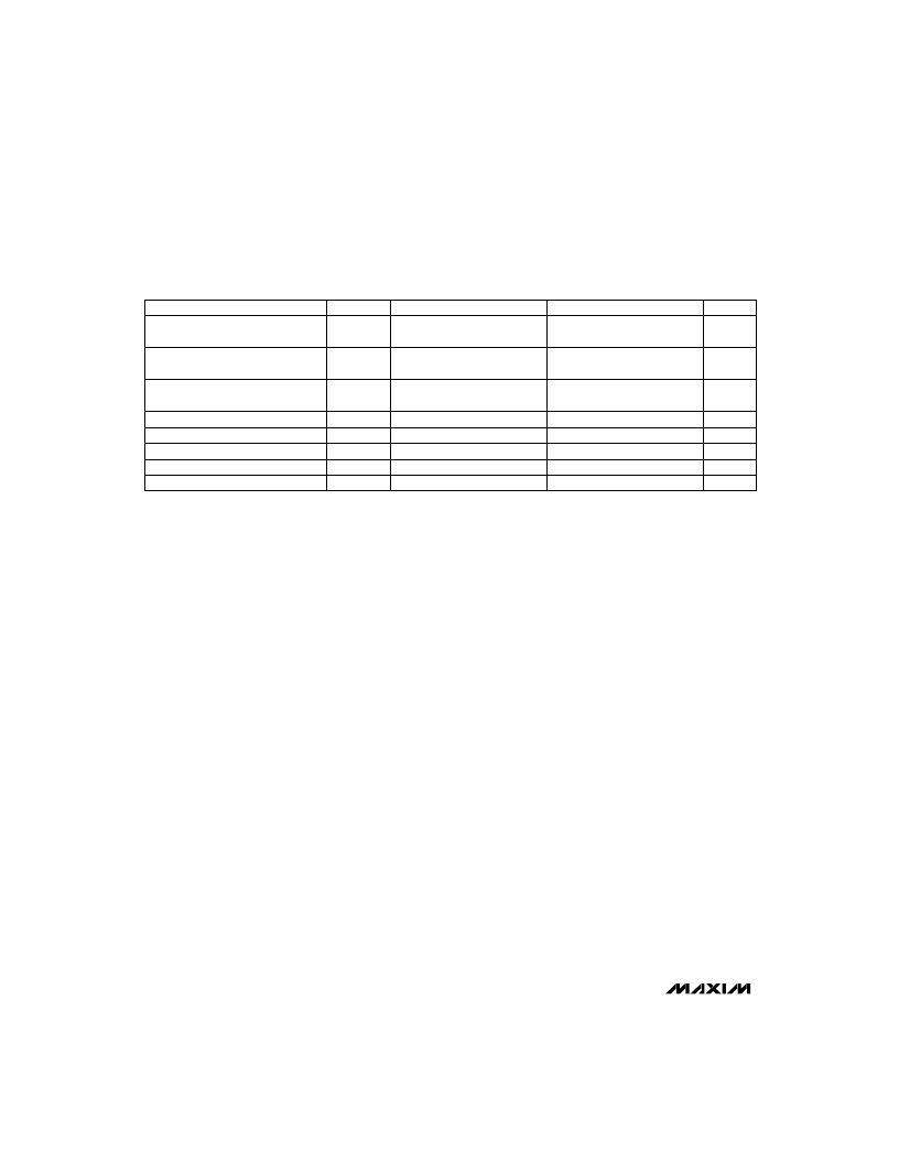
PARAMETER
SYMBOL
CONDITIONS
MIN
TYP
MAX
UNITS
Propagation Delay
t
PD+,
t
PD-
V
IN
= 100mV, V
OD
= 5mV
(Note 9)
45
70
ns
Differential Propagation Delay
t
PD
V
IN
= 100mV, V
OD
= 5mV
(Note 10)
2
ns
Propagation Delay Skew
t
PD
skew
MAX909 only: V
IN
= 100mV,
V
OD
= 5mV (Note 11)
4
ns
Latch Input Voltage High
Latch Input Voltage Low
Latch Input Current
Latch Setup Time
V
IH
V
IL
I
IH
, I
IL
t
s
(Note 12)
(Note 12)
(Note 12)
(Note 12)
2.0
V
V
Latch Hold Time
t
h
(Note 12)
4
ns
0.8
20
μA
ns
4
相關(guān)PDF資料 |
PDF描述 |
|---|---|
| MAX9075EXK-T | Low-Cost, Ultra-Small, 3レA Single-Supply Comparators |
| MAX9077EKA-T | Low-Cost, Ultra-Small, 3レA Single-Supply Comparators |
| MAX9075 | Low-Cost, Ultra-Small, 3レA Single-Supply Comparators |
| MAX9075EUK-T | Low-Cost, Ultra-Small, 3レA Single-Supply Comparators |
| MAX9077 | Low-Cost, Ultra-Small, 3レA Single-Supply Comparators |
相關(guān)代理商/技術(shù)參數(shù) |
參數(shù)描述 |
|---|---|
| MAX910 | 制造商:MAXIM 制造商全稱:Maxim Integrated Products 功能描述: |
| MAX910/MAX911 | 制造商:MAXIM 制造商全稱:Maxim Integrated Products 功能描述:High-Speed Threshold-Programmable Voltage Comparators |
| MAX9100 | 制造商:MAXIM 制造商全稱:Maxim Integrated Products 功能描述:+1.0V Micropower SOT23 Comparators |
| MAX9100_07 | 制造商:MAXIM 制造商全稱:Maxim Integrated Products 功能描述:+1.0V Micropower SOT23 Comparators |
| MAX9100ESA | 功能描述:校驗(yàn)器 IC 1.0V uPower Comparator RoHS:否 制造商:STMicroelectronics 產(chǎn)品: 比較器類型: 通道數(shù)量: 輸出類型:Push-Pull 電源電壓-最大:5.5 V 電源電壓-最小:1.1 V 補(bǔ)償電壓(最大值):6 mV 電源電流(最大值):1350 nA 響應(yīng)時(shí)間: 最大工作溫度:+ 125 C 安裝風(fēng)格:SMD/SMT 封裝 / 箱體:SC-70-5 封裝:Reel |
發(fā)布緊急采購,3分鐘左右您將得到回復(fù)。