- 您現在的位置:買賣IC網 > PDF目錄383513 > MAX8808XETA (MAXIM INTEGRATED PRODUCTS INC) 1A Linear Li+ Battery Chargers with Integrated Pass FET and Thermal Regulation in 2mm x 2mm TDFN PDF資料下載
參數資料
| 型號: | MAX8808XETA |
| 廠商: | MAXIM INTEGRATED PRODUCTS INC |
| 元件分類: | 電源管理 |
| 英文描述: | 1A Linear Li+ Battery Chargers with Integrated Pass FET and Thermal Regulation in 2mm x 2mm TDFN |
| 中文描述: | 1-CHANNEL POWER SUPPLY SUPPORT CKT, DSO8 |
| 封裝: | 2 X 2 MM, 0.80 HEIGHT, MO-229, TDFN-8 |
| 文件頁數: | 2/13頁 |
| 文件大小: | 236K |
| 代理商: | MAX8808XETA |
M
1A Linear Li+ Battery Chargers with Integrated Pass
FET and Thermal Regulation in 2mm x 2mm TDFN
2
_______________________________________________________________________________________
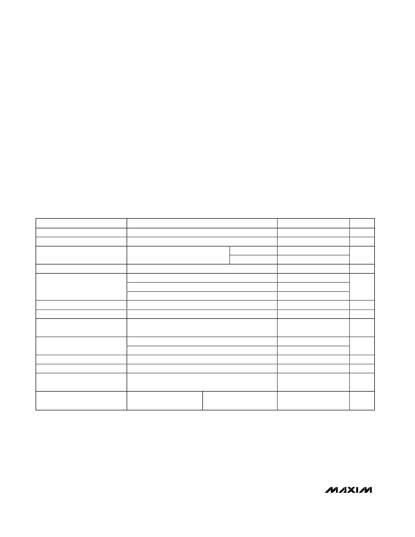
ABSOLUTE MAXIMUM RATINGS
IN to GND...............................................................-0.3V to +16V
VL, BATT,
EN
,
ACOK
,
CHG
to GND.........................-0.3V to +6V
VL, ISET to GND.......................................................-0.3V to +4V
VL to IN................................................................-16.3V to +0.3V
IN to BATT Continuous Current.............................................1.5A
Continuous Power Dissipation (T
A
= +70°C)
8-Pin 2mm x 2mm TDFN (derate 15.4mW/°C
above +70°C).............................................................1234mW
ELECTRICAL CHARACTERISTICS
(V
IN
= 5V, V
BATT
= 4.0V, R
ACOK
= R
CHG
= 100k
to 5V,
EN
= unconnected (for the MAX8808X and MAX8808Z), EN = VL (for the
MAX8808Y), R
ISET
= 2.8k
to GND, C
VL
= 0.47μF, C
BATT
= 1μF, T
A
= -40°C to +85°C, unless otherwise noted. Typical values are at
T
A
= +25°C.)(Note 1)
Stresses beyond those listed under “Absolute Maximum Ratings” may cause permanent damage to the device. These are stress ratings only, and functional
operation of the device at these or any other conditions beyond those indicated in the operational sections of the specifications is not implied. Exposure to
absolute maximum rating conditions for extended periods may affect device reliability.
BATT Short-Circuit Duration.......................................Continuous
Operating Temperature Range ...........................-40°C to +85°C
Junction Temperature......................................................+150°C
Storage Temperature Range.............................-65°C to +150°C
Lead Temperature (soldering, 10s).................................+300°C
PARAMETER
CONDITIONS
MIN
0
4.25
15
10
6.5
TYP
MAX
15
6.50
60
45
7.5
2
0.50
0.065
UNITS
V
V
Input Voltage Range
Input Operating Range
V
IN
rising
V
IN
falling
40
30
7
0.8
0.23
ACOK
Threshold
V
IN
- V
BATT
, 10mV hysteresis (typ)
mV
Overvoltage-Lockout Trip Point
V
IN
rising, 100mV hysteresis (typ)
Charging (I
IN
- I
BATT
)
Disabled
OFF state (V
IN
= V
BATT
= 4.0V)
I
VL
= 100μA
I
VL
= 100μA to 2mA
V
IN Input Current
mA
VL Output Voltage
VL Load Regulation
3.0
-5
V
-30
mV
VL Undervoltage-Lockout Trip
Point
V
VL
rising, 100mV hysteresis (typ)
2.74
V
V
IN
= 0 to 4V
Disabled
1
1
10
10
BATT Input Current
μA
Maximum RMS Charge Current
Battery Regulation Voltage
1
A
RMS
V
I
BATT
= 1mA
4.162
4.200
4.238
Minimum BATT Bypass
Capacitance
2.2
μF/A
Fast-Charge Current Loop
System Accuracy
V
BATT
= 3.5V
T
A
= 0°C to +85°C
418
465
512
mA
相關PDF資料 |
PDF描述 |
|---|---|
| MAX881REVKIT | Evaluation Kit for the MAX881R |
| MAX8890EGCBFK | Analog IC |
| MAX8890EGCBFL | Analog IC |
| MAX8890EGCBFM | Analog IC |
| MAX8890EGCBGA | Analog IC |
相關代理商/技術參數 |
參數描述 |
|---|---|
| MAX8808XETA+ | 制造商:Maxim Integrated Products 功能描述:CHRGR LI-ION/LI-POL 1000MA 4.2V 8TDFN EP - Rail/Tube |
| MAX8808XETA+T | 功能描述:電池管理 1A Linear Li+ Battery Charger RoHS:否 制造商:Texas Instruments 電池類型:Li-Ion 輸出電壓:5 V 輸出電流:4.5 A 工作電源電壓:3.9 V to 17 V 最大工作溫度:+ 85 C 最小工作溫度:- 40 C 封裝 / 箱體:VQFN-24 封裝:Reel |
| MAX8808XETA+TG104 | 功能描述:電池管理 1A Linear Li+ Battery Charger RoHS:否 制造商:Texas Instruments 電池類型:Li-Ion 輸出電壓:5 V 輸出電流:4.5 A 工作電源電壓:3.9 V to 17 V 最大工作溫度:+ 85 C 最小工作溫度:- 40 C 封裝 / 箱體:VQFN-24 封裝:Reel |
| MAX8808XETA-T | 功能描述:電池管理 RoHS:否 制造商:Texas Instruments 電池類型:Li-Ion 輸出電壓:5 V 輸出電流:4.5 A 工作電源電壓:3.9 V to 17 V 最大工作溫度:+ 85 C 最小工作溫度:- 40 C 封裝 / 箱體:VQFN-24 封裝:Reel |
| MAX8808YETA | 制造商:Maxim Integrated Products 功能描述:1A LINEAR LI+ BATT CHRGRS W. INTEG - Rail/Tube |
發(fā)布緊急采購,3分鐘左右您將得到回復。