- 您現(xiàn)在的位置:買(mǎi)賣(mài)IC網(wǎng) > PDF目錄383513 > MAX8740 (Maxim Integrated Products, Inc.) TFT-LCD Step-Up DC-DC Converter PDF資料下載
參數(shù)資料
| 型號(hào): | MAX8740 |
| 廠商: | Maxim Integrated Products, Inc. |
| 元件分類(lèi): | DC/DC變換器 |
| 英文描述: | TFT-LCD Step-Up DC-DC Converter |
| 中文描述: | TFT-LCD升壓型DC-DC轉(zhuǎn)換器 |
| 文件頁(yè)數(shù): | 2/12頁(yè) |
| 文件大小: | 341K |
| 代理商: | MAX8740 |
M
TFT-LCD Step-Up DC-DC Converter
2
_______________________________________________________________________________________
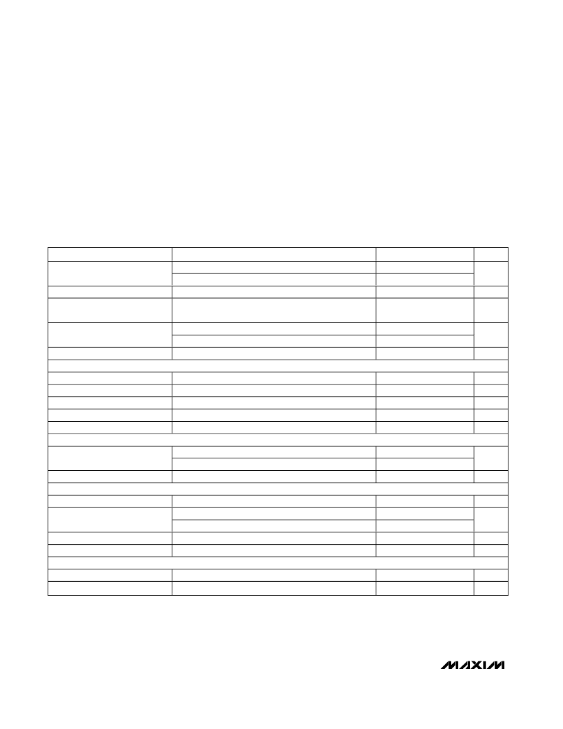
ABSOLUTE MAXIMUM RATINGS
LX to GND ..............................................................-0.3V to +30V
IN,
SHDN
, FREQ, FB to GND...................................-0.3V to +6V
COMP, SS to GND.......................................-0.3V to (V
IN
+ 0.3V)
LX Switch Maximum Continuous RMS Current.....................2.4A
Continuous Power Dissipation (T
A
= +70
°
C)
10-Pin TDFN (derate 24.1mW/
°
C above +70
°
C).......1481.5mW
ELECTRICAL CHARACTERISTICS
(V
IN
= V
SHDN
= 3V,
T
A
= 0°C to +85°C
. Typical values are at T
A
= +25°C, unless otherwise noted.)
Stresses beyond those listed under “Absolute Maximum Ratings” may cause permanent damage to the device. These are stress ratings only, and functional
operation of the device at these or any other conditions beyond those indicated in the operational sections of the specifications is not implied. Exposure to
absolute maximum rating conditions for extended periods may affect device reliability.
Operating Temperature Range ...........................-40
°
C to +85
°
C
Junction Temperature......................................................+150
°
C
Storage Temperature Range.............................-65
°
C to +160
°
C
Lead Temperature (soldering, 10s).................................+300
°
C
PARAMETER
CONDITIONS
MIN
2.6
4.0
TYP
MAX
5.5
5.5
28
UNITS
V
OUT
< 18V
18V < V
OUT
< 24V
Input Voltage Range
V
Output Voltage Range
V
IN Undervoltage-Lockout
Threshold
V
IN
rising, typical hysteresis is 50mV; LX remains off
below this level
2.20
2.38
2.57
V
V
FB
= 1.3V, not switching
V
FB
= 1.0V, switching, FREQ = GND
SHDN
= GND
0.22
2
0.1
0.44
5
10.0
IN Quiescent Current
mA
IN Shutdown Current
ERROR AMPLIFIER
FB Regulation Voltage
FB Input Bias Current
FB Line Regulation
Transconductance
Voltage Gain
OSCILLATOR
μA
Level to produce V
COMP
= 1.24V
V
FB
= 1.24V
Level to produce V
COMP
= 1.24V, V
IN
= 2.6V to 5.5V
1.22
50
1.24
125
0.05
200
2400
1.26
250
0.15
315
V
nA
%/V
μS
V/V
100
FREQ = GND
FREQ = IN
540
1000
88
640
1220
91
740
1500
94
Frequency
kHz
Maximum Duty Cycle
n-CHANNEL MOSFET
Current Limit
%
V
FB
= 1V, 71% duty cycle
V
IN
= 3V (typ value at T
A
= +25°C)
V
IN
= 5V (typ value at T
A
= +25°C)
V
LX
= 28V
3.9
4.6
0.11
0.095
30
0.15
5.3
0.17
0.15
55
0.25
A
On-Resistance
Leakage Current
Current-Sense Transresistance
SOFT-START
Reset Switch Resistance
Charge Current
μA
V/A
0.09
100
7.5
μA
V
SS
= 1.2V
2.5
4.5
相關(guān)PDF資料 |
PDF描述 |
|---|---|
| MAX8740ETB | TFT-LCD Step-Up DC-DC Converter |
| MAX878LCPA | Analog IC |
| MAX8710 | LCD display panel power supply TFT Monitor TV |
| MAX8711 | LCD display panel power supply TFT Monitor TV |
| MAX8712 | LCD display panel power supply TFT Monitor TV |
相關(guān)代理商/技術(shù)參數(shù) |
參數(shù)描述 |
|---|---|
| MAX8740ETB | 制造商:Maxim Integrated Products 功能描述:LOW COST LCD MONITOR PANEL POWER SU - Rail/Tube |
| MAX8740ETB+ | 制造商:Maxim Integrated Products 功能描述:- Rail/Tube |
| MAX8740ETB+T | 功能描述:LCD 驅(qū)動(dòng)器 TFT-LCD Step-Up DC/DC Converter RoHS:否 制造商:Maxim Integrated 數(shù)位數(shù)量:4.5 片段數(shù)量:30 最大時(shí)鐘頻率:19 KHz 工作電源電壓:3 V to 3.6 V 最大工作溫度:+ 85 C 最小工作溫度:- 20 C 封裝 / 箱體:PDIP-40 封裝:Tube |
| MAX8740ETB-T | 功能描述:LCD 驅(qū)動(dòng)器 RoHS:否 制造商:Maxim Integrated 數(shù)位數(shù)量:4.5 片段數(shù)量:30 最大時(shí)鐘頻率:19 KHz 工作電源電壓:3 V to 3.6 V 最大工作溫度:+ 85 C 最小工作溫度:- 20 C 封裝 / 箱體:PDIP-40 封裝:Tube |
| MAX8740EUB+ | 制造商:Maxim Integrated Products 功能描述:- Rail/Tube |
發(fā)布緊急采購(gòu),3分鐘左右您將得到回復(fù)。