- 您現(xiàn)在的位置:買賣IC網(wǎng) > PDF目錄383512 > MAX861ISA (MAXIM INTEGRATED PRODUCTS INC) Quadruple 2-Input Positive-NOR Gates 14-CFP -55 to 125 PDF資料下載
參數(shù)資料
| 型號(hào): | MAX861ISA |
| 廠商: | MAXIM INTEGRATED PRODUCTS INC |
| 元件分類: | 穩(wěn)壓器 |
| 英文描述: | Quadruple 2-Input Positive-NOR Gates 14-CFP -55 to 125 |
| 中文描述: | SWITCHED CAPACITOR CONVERTER, 250 kHz SWITCHING FREQ-MAX, PDSO8 |
| 封裝: | 0.150 INCH, PLASTIC, SOIC-8 |
| 文件頁(yè)數(shù): | 6/12頁(yè) |
| 文件大小: | 142K |
| 代理商: | MAX861ISA |
_______________Detailed Desc ription
The MAX860/MAX861 capacitive charge pumps either
invert or double the voltage applied to their inputs. For
highest performance, use low equivalent series resis-
tance (ESR) capacitors. See the Capacitor Selection
section for more details. The frequency-control (FC) pin
allows you to choose one of three switching frequen-
cies; these three selectable frequencies are different for
each device. When shut down, MAX860/MAX861 cur-
rent consumption reduces to less than 1μA.
Common Applic ations
Voltage Inverter
The most common application for these devices is a
charge-pump voltage inverter (see Typical Operating
Circuits). This application requires only two external com-
ponents—capacitors C1 and C2—plus a bypass capacitor
if necessary (see Bypass Capacitor section). Refer to the
Capacitor Selectionsection for suggested capacitor types
and values.
Even though the MAX860/MAX861’s output is not actively
regulated, it is fairly insensitive to load-current changes. A
circuit output source resistance of 12
(calculated using
the formula given in the Capacitor Selection section)
means that, with a +5V input, the output voltage is -5V
under no load and decreases to -4.4V with a 50mA load.
The MAX860/MAX861 output source resistance (used to
calculate the circuit output source resistance) vs. tempera-
ture and supply voltage are shown in the Typical
Operating Characteristicsgraphs.
Calculate the output ripple voltage using the formula
given in the Capacitor Selectionsection.
Positive Voltage Doubler
The MAX860/MAX861 can also operate as positive volt-
age doublers (see Typical Operating Circuits). This
application requires only two external components,
capacitors C1 and C2. The no-load output is twice the
input voltage. The electrical specifications in the doubler
mode are very similar to those of the inverter mode
except for the Supply Voltage Range (see Electrical
Characteristics table) and No-Load Supply Current (see
graph in Typical Operating Characteristics). The circuit
output source resistance and output ripple voltage are
calculated using the formulas in the Capacitor Selection
section.
When driven low, the –———N
device. In inverter mode, conneinput shuts down the
not used. In doubler mode, connect –———Nto G if it is
is not used. When the device is shut down, all active
circuitry is turned off.
In the inverting configuration, loads connected from
OUT to GND are not powered in shutdown mode.
However, a reverse-current path exists through two
diodes between OUT and GND; therefore, loads con-
nected from V
DD
to OUT draw current from the input
supply.
In the doubling configuration, loads connected from the
V
DD
pin to the GND pin are not powered in shutdown
mode. Loads connected from the V
DD
pin to the OUT
pin draw current from the input supply through a path
similar to that of the inverting configuration (described
above).
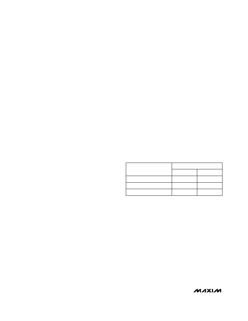
Frequenc y Control
Charge-pump frequency for both devices can be set to
one of three values. Each device has a unique set of
three available frequencies, as indicated in Table 1.
The oscillator and charge-pump frequencies are the
same (i.e., the charge-pump frequency is not half the
oscillator frequency, as it is on the MAX660, MAX665,
and ICL7660).
*See the Electrical Characteristics for detailed switching-
frequency specifications.
A higher switching frequency minimizes capacitor size
for the same performance and increases the supply
current (Table 2). The lowest fundamental frequency of
the switching noise is equal to the minimum specified
switching frequency (e.g., 3kHz for the MAX860 with FC
open). The spectrum of noise frequencies extends
above this value because of harmonics in the switching
waveform. To get best noise performance, choose the
device and FC connection to select a minimum switch-
ing frequency that lies above your sensitive bandwidth.
Low-Voltage-Operation Input
LV should be connected to GND for inverting operation.
To enhance compatibility with the MAX660, MAX665, and
ICL7660, you may float LV if the input voltage exceeds 3V.
In doubling mode, LV must be connected to OUT for all
input voltages.
M
50mA, Frequenc y-S elec table,
S witc hed-Capac itor Voltage Converters
6
_______________________________________________________________________________________
FREQUENCY (kHz)
FC CONNECTION
MAX860
MAX861
FC = V
DD
or open
6
13
FC = GND
50
100
FC = OUT
130
250
Table 1. Nominal Switching Frequencies*
相關(guān)PDF資料 |
PDF描述 |
|---|---|
| MAX861MJA | 50mA, Frequency-Selectable, Switched-Capacitor Voltage Converters |
| MAX872-MAX874 | 10レA, Low-Dropout, Precision Voltage References |
| MAX872CPA | 8-Bit Identity/Magnitude Comparators (P=Q) with Enable 20-CFP -55 to 125 |
| MAX872CSA | 8-Bit Identity/Magnitude Comparators (P=Q) with Enable 20-CDIP -55 to 125 |
| MAX872EPA | 8-Bit Identity/Magnitude Comparators (P=Q) with Enable 20-LCCC -55 to 125 |
相關(guān)代理商/技術(shù)參數(shù) |
參數(shù)描述 |
|---|---|
| MAX861ISA+ | 功能描述:電荷泵 50mA f-Selectable Switched-Cap V Conv RoHS:否 制造商:Maxim Integrated 功能:Inverting, Step Up 輸出電壓:- 1.5 V to - 5.5 V, 3 V to 11 V 輸出電流:100 mA 電源電流:1 mA 最大工作溫度:+ 70 C 封裝 / 箱體:SOIC-8 Narrow 封裝:Tube |
| MAX861ISA+T | 功能描述:電荷泵 50mA f-Selectable Switched-Cap V Conv RoHS:否 制造商:Maxim Integrated 功能:Inverting, Step Up 輸出電壓:- 1.5 V to - 5.5 V, 3 V to 11 V 輸出電流:100 mA 電源電流:1 mA 最大工作溫度:+ 70 C 封裝 / 箱體:SOIC-8 Narrow 封裝:Tube |
| MAX861ISA-T | 功能描述:電荷泵 50mA f-Selectable Switched-Cap V Conv RoHS:否 制造商:Maxim Integrated 功能:Inverting, Step Up 輸出電壓:- 1.5 V to - 5.5 V, 3 V to 11 V 輸出電流:100 mA 電源電流:1 mA 最大工作溫度:+ 70 C 封裝 / 箱體:SOIC-8 Narrow 封裝:Tube |
| MAX861ISA-TG069 | 制造商:Rochester Electronics LLC 功能描述: 制造商:Maxim Integrated Products 功能描述: |
| MAX861IUA | 功能描述:電荷泵 50mA f-Selectable Switched-Cap V Conv RoHS:否 制造商:Maxim Integrated 功能:Inverting, Step Up 輸出電壓:- 1.5 V to - 5.5 V, 3 V to 11 V 輸出電流:100 mA 電源電流:1 mA 最大工作溫度:+ 70 C 封裝 / 箱體:SOIC-8 Narrow 封裝:Tube |
發(fā)布緊急采購(gòu),3分鐘左右您將得到回復(fù)。