- 您現(xiàn)在的位置:買賣IC網(wǎng) > PDF目錄385553 > MAX8531EBT (Maxim Integrated Products, Inc.) Dual Low-Dropout Linear Regulators with RESETor Low-Noise Output in UCSP or QFN PDF資料下載
參數(shù)資料
| 型號: | MAX8531EBT |
| 廠商: | Maxim Integrated Products, Inc. |
| 英文描述: | Dual Low-Dropout Linear Regulators with RESETor Low-Noise Output in UCSP or QFN |
| 中文描述: | 雙低壓差線性穩(wěn)壓器與RESETor低噪聲的輸出UCSP或QFN封裝 |
| 文件頁數(shù): | 7/12頁 |
| 文件大小: | 280K |
| 代理商: | MAX8531EBT |
Shutdown
The MAX8530/MAX8531 have a single shutdown con-
trol input (
SHDN
). Drive
SHDN
low to shut down both
outputs, reducing supply current to 10nA. Connect
SHDN
to a logic high, or IN, for normal operation.
Internal P-Channel Pass Transistor
The MAX8530/MAX8531 feature two 1
P-channel
MOSFET pass transistors. A P-channel MOSFET pro-
vides several advantages over similar designs using
PNP pass transistors, including longer battery life. It
requires no base drive, substantially reducing quies-
cent current. PNP-based regulators waste considerable
current in dropout when the pass transistor saturates
and also use high base-drive currents under heavy
loads. The MAX8530/MAX8531 do not suffer these
problems and consume only 150μA of quiescent cur-
rent whether in dropout, light-load, or heavy-load appli-
cations (see the
Typical Operating Characteristics
).
Whereas a PNP-based regulator has dropout voltage
that is independent of the load, a P-channel MOSFET
’
s
dropout voltage is proportional to load current, providing
for low dropout voltage at heavy loads and extremely
low dropout voltage at lighter loads.
Current Limit
The MAX8530/MAX8531 contain two independent cur-
rent limiters, one for each regulator, which monitor and
control the pass transistor
’
s gate voltage and limit the
output currents to 210mA and 165mA minimum. The
output can be shorted to ground for an indefinite time
without damaging the part.
Thermal-Overload Protection
Thermal-overload protection limits total power dissipa-
tion in the MAX8530/MAX8531. When the junction tem-
perature exceeds T
J
= +160
°
C, the thermal sensor
signals the shutdown logic, turning off the pass transistor
and allowing the IC to cool. The thermal sensor turns the
pass transistor on again after the IC
’
s junction tempera-
ture cools by 10
°
C, resulting in a pulsed output during
continuous thermal-overload conditions.
Thermal-overload protection is designed to protect the
MAX8530/MAX8531 in the event of fault conditions. For
continual operation, do not exceed the absolute maxi-
mum junction temperature rating of T
J
= +150
°
C.
Operating Region and Power Dissipation
The MAX8530/MAX8531s
’
maximum power dissipation
depends on the thermal resistance of the case and cir-
cuit board, the temperature difference between the die
junction and ambient air, and the rate of airflow. The
power dissipation across the device is P = I
OUT
(V
IN
-
V
OUT
). Maximum power dissipation:
P
MAX
= (T
J
- T
A
)/(
θ
JB
+
θ
BA
)
where T
J
- T
A
is the temperature difference between the
MAX8530/MAX8531 die junction and the surrounding air,
θ
JB
(or
θ
JC
) is the thermal resistance of the package, and
θ
BA
is the thermal resistance through the printed circuit
board, copper traces, and other materials to the sur-
rounding air.
The GND pin of the MAX853_ETT__ (6-lead QFN) per-
forms the dual functions of providing an electrical con-
nection to the ground and channeling heat away.
Connect the GND pin and exposed pad to ground
using a large pad or ground plane.
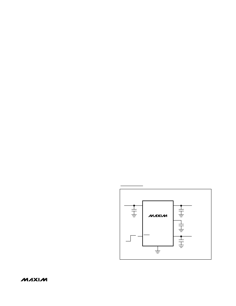
Low-Noise Operation (MAX8531)
An external 0.01μF bypass capacitor at BP, in conjunc-
tion with an internal resistor, creates a lowpass filter
(see the
Typical Application Circuit
). The MAX8531
exhibits 40μV
RMS
output voltage noise with C
BP
=
0.01μF and C
OUT
= 2.2μF (see the Output Noise
Spectral Density vs. Frequency graph in the
Typical
Operating Characteristics
).
M
Dual Low-Dropout Linear Regulators
with
RESET
or Low-Noise Output in UCSP or QFN
_______________________________________________________________________________________
7
IN
OUT1
2.2
μ
F
C
IN
2.2
μ
F
INPUT
2.5V TO 6.5V
1.5V TO 3.3V
AT 200mA
1.5V TO 3.3V
AT 150mA
1
μ
F
10nF
SHDN
OFF
ON
OUT2
GND
BP
MAX8531
MAX8531
Typical Appication Circuit
相關PDF資料 |
PDF描述 |
|---|---|
| MAX8531ETT | Dual Low-Dropout Linear Regulators with RESETor Low-Noise Output in UCSP or QFN |
| MAX853 | Charge-Pump Power Supplies for GaAsFET Bias(可調(diào),砷化鎵場效應管偏置電壓源) |
| MAX858 | Step-Up DC-DC Converters(可調(diào)節(jié)輸出,高效率,低IQ值,步升DC-DC變換器) |
| MAX860CSA | DC-to-DC Voltage Converter |
| MAX860CUA | DC-to-DC Voltage Converter |
相關代理商/技術參數(shù) |
參數(shù)描述 |
|---|---|
| MAX8531EBTA8 | 制造商:Maxim Integrated Products 功能描述:DUAL LOW-DROPOUT LINEAR REGULATORS - Rail/Tube |
| MAX8531EBTA8-T | 功能描述:低壓差穩(wěn)壓器 - LDO Dual Low-Dropout Linear Regulator RoHS:否 制造商:Texas Instruments 最大輸入電壓:36 V 輸出電壓:1.4 V to 20.5 V 回動電壓(最大值):307 mV 輸出電流:1 A 負載調(diào)節(jié):0.3 % 輸出端數(shù)量: 輸出類型:Fixed 最大工作溫度:+ 125 C 安裝風格:SMD/SMT 封裝 / 箱體:VQFN-20 |
| MAX8531EBTGG | 制造商:Rochester Electronics LLC 功能描述: 制造商:Maxim Integrated Products 功能描述: |
| MAX8531EBTGG+T | 功能描述:低壓差穩(wěn)壓器 - LDO Dual Low-Dropout Linear Regulator RoHS:否 制造商:Texas Instruments 最大輸入電壓:36 V 輸出電壓:1.4 V to 20.5 V 回動電壓(最大值):307 mV 輸出電流:1 A 負載調(diào)節(jié):0.3 % 輸出端數(shù)量: 輸出類型:Fixed 最大工作溫度:+ 125 C 安裝風格:SMD/SMT 封裝 / 箱體:VQFN-20 |
| MAX8531EBTGGJ+T | 功能描述:低壓差穩(wěn)壓器 - LDO Dual Low-Dropout Linear Regulator RoHS:否 制造商:Texas Instruments 最大輸入電壓:36 V 輸出電壓:1.4 V to 20.5 V 回動電壓(最大值):307 mV 輸出電流:1 A 負載調(diào)節(jié):0.3 % 輸出端數(shù)量: 輸出類型:Fixed 最大工作溫度:+ 125 C 安裝風格:SMD/SMT 封裝 / 箱體:VQFN-20 |
發(fā)布緊急采購,3分鐘左右您將得到回復。