- 您現(xiàn)在的位置:買賣IC網(wǎng) > PDF目錄384705 > MAX809LTRG (ON SEMICONDUCTOR) Very Low Supply Current 3−Pin Microprocessor Reset Monitors PDF資料下載
參數(shù)資料
| 型號: | MAX809LTRG |
| 廠商: | ON SEMICONDUCTOR |
| 元件分類: | 電源管理 |
| 英文描述: | Very Low Supply Current 3−Pin Microprocessor Reset Monitors |
| 中文描述: | 1-CHANNEL POWER SUPPLY SUPPORT CKT, PDSO3 |
| 封裝: | LEAD FREE, TO-236, SOT-23, 3 PIN |
| 文件頁數(shù): | 7/11頁 |
| 文件大小: | 93K |
| 代理商: | MAX809LTRG |
MAX809 Series, MAX810 Series
http://onsemi.com
7
APPLICATIONS INFORMATION
V
CC
Transient Rejection
The MAX809 provides accurate V
CC
monitoring and
reset timing during powerup, powerdown, and
brownout/sag conditions, and rejects negativegoing
transients (glitches) on the power supply line. Figure 13
shows the maximum transient duration vs. maximum
negative excursion (overdrive) for glitch rejection. Any
combination of duration and overdrive which lies
under
the
curve will
not
generate a reset signal. Combinations above
the curve are detected as a brownout or powerdown.
Typically, transient that goes 100 mV below the reset
threshold and lasts 5.0 s or less will not cause a reset pulse.
Transient immunity can be improved by adding a capacitor
in close proximity to the V
CC
pin of the MAX809.
Figure 13. Maximum Transient Duration vs.
Overdrive for Glitch Rejection at 25
°
C
Duration
V
TH
Overdrive
V
CC
10
250
200
110
60
RESET COMPARATOR OVERDRIVE (mV)
M
50
300
0
410
V
TH
= 4.9 V
150
100
V
TH
= 1.2 V
160
210
260
310
360
V
TH
= 2.93 V
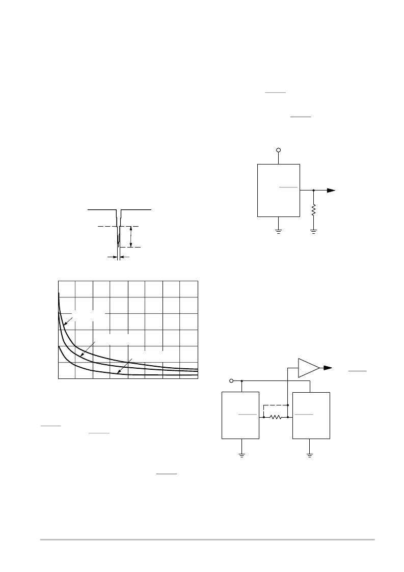
RESET Signal Integrity During PowerDown
The MAX809 RESET output is valid to V
CC
= 1.0 V.
Below this voltage the output becomes an “open circuit” and
does not sink current. This means CMOS logic inputs to the
Microprocessor will be floating at an undetermined voltage.
Most digital systems are completely shutdown well above
this voltage. However, in situations where RESET must be
maintained valid to V
CC
= 0 V, a pulldown resistor must be
connected from RESET to ground to discharge stray
capacitances and hold the output low (Figure 14). This
resistor value, though not critical, should be chosen such that
it does not appreciably load RESET under normal operation
(100 k will be suitable for most applications).
V
CC
V
CC
RESET
RESET
R1
100 k
MAX809/810
GND
Figure 14. Ensuring RESET Valid to V
CC
= 0 V
Processors With Bidirectional I/O Pins
Some Microprocessor’s have bidirectional reset pins.
Depending on the current drive capability of the processor
pin, an indeterminate logic level may result if there is a logic
conflict. This can be avoided by adding a 4.7 k resistor in
series with the output of the MAX809 (Figure 15). If there
are other components in the system which require a reset
signal, they should be buffered so as not to load the reset line.
If the other components are required to follow the reset I/O
of the Microprocessor, the buffer should be connected as
shown with the solid line.
V
CC
V
CC
Microprocessor
RESET
RESET
MAX809/810
GND
GND
4.7 k
Figure 15. Interfacing to Bidirectional Reset I/O
RESET
V
CC
BUFFERED RESET
TO OTHER SYSTEM
COMPONENTS
BUFFER
相關PDF資料 |
PDF描述 |
|---|---|
| MAX809MTRG | Very Low Supply Current 3−Pin Microprocessor Reset Monitors |
| MAX809RTRG | Very Low Supply Current 3−Pin Microprocessor Reset Monitors |
| MAX809SN120T1G | Very Low Supply Current 3−Pin Microprocessor Reset Monitors |
| MAX809SN160T1G | Very Low Supply Current 3−Pin Microprocessor Reset Monitors |
| MAX809SN232T1G | Very Low Supply Current 3−Pin Microprocessor Reset Monitors |
相關代理商/技術(shù)參數(shù) |
參數(shù)描述 |
|---|---|
| MAX809LTRG-CUT TAPE | 制造商:ON 功能描述:MAX809 Series 4.63 V 140 ms 3-Pin Microprocessor Reset Monitor - SOT-23-3 |
| MAX809LW | 制造商:PHILIPS 制造商全稱:NXP Semiconductors 功能描述:3-pin microprocessor resets |
| MAX809M | 制造商:Maxim Integrated Products 功能描述:3-PIN MICROPROCESSOR RESET MONITOR |
| MAX809MCPA | 制造商:MAXIM 制造商全稱:Maxim Integrated Products 功能描述:Voltage Detector |
| MAX809MCUR | 制造商:MAXIM 制造商全稱:Maxim Integrated Products 功能描述:Voltage Detector |
發(fā)布緊急采購,3分鐘左右您將得到回復。