- 您現(xiàn)在的位置:買賣IC網(wǎng) > PDF目錄383502 > MAX783CBX (MAXIM INTEGRATED PRODUCTS INC) Modular Connector; No. of Contacts:8; No. of Ports:1; LAN Category:5; Leaded Process Compatible:Yes; Peak Reflow Compatible (260 C):No RoHS Compliant: Yes PDF資料下載
參數(shù)資料
| 型號(hào): | MAX783CBX |
| 廠商: | MAXIM INTEGRATED PRODUCTS INC |
| 元件分類: | 穩(wěn)壓器 |
| 英文描述: | Modular Connector; No. of Contacts:8; No. of Ports:1; LAN Category:5; Leaded Process Compatible:Yes; Peak Reflow Compatible (260 C):No RoHS Compliant: Yes |
| 中文描述: | DUAL SWITCHING CONTROLLER, 330 kHz SWITCHING FREQ-MAX, PDSO36 |
| 封裝: | PLASTIC, SSOP-36 |
| 文件頁數(shù): | 12/28頁 |
| 文件大?。?/td> | 279K |
| 代理商: | MAX783CBX |
第1頁第2頁第3頁第4頁第5頁第6頁第7頁第8頁第9頁第10頁第11頁當(dāng)前第12頁第13頁第14頁第15頁第16頁第17頁第18頁第19頁第20頁第21頁第22頁第23頁第24頁第25頁第26頁第27頁第28頁
M
Triple-Output Power-S upply Controller
for Notebook Computers
12
______________________________________________________________________________________
Soft-Start/SS_ Inputs
Connecting capacitors to SS3 and SS5 allows gradual
build-up of the +3.3V and +5V supplies after ON3 and
ON5 are driven high. When ON3 or ON5 is low, the
appropriate SS capacitors are discharged to GND.
When ON3 or ON5 is driven high, a 4μA constant cur-
rent source charges these capacitors up to 4V. The
resulting ramp voltage on the SS_ pins linearly increas-
es the current-limit comparator setpoint so as to
increase the duty cycle to the external power MOSFETs
up to the maximum output. With no SS capacitors, the
circuit will reach maximum current limit within 10μs.
Soft-start greatly reduces initial in-rush current peaks
and allows start-up time to be programmed externally.
Synchronous Rectifiers
Synchronous rectification allows for high efficiency by
reducing the losses associated with the Schottky recti-
fiers. Also, the synchronous rectifier MOSFETS are
necessary for correct operation of the MAX783's boost
gate-drive and VDD supplies.
When the external high-side power MOSFET turns off,
energy stored in the inductor causes its terminal volt-
age to reverse instantly. Current flows in the loop
formed by the inductor, Schottky diode, and load—an
action that charges up the filter capacitor. The Schottky
diode has a forward voltage of about 0.5V which,
although small, represents a significant power loss and
degrades efficiency. A synchronous rectifier MOSFET
parallels the diode and is turned on by DL3 (or DL5)
shortly after the diode conducts. Since the on resis-
tance (r
) of the synchronous rectifier is very low,
the losses are reduced.
The synchronous rectifier MOSFET is turned off when
the inductor current falls to zero.
Cross conduction (or “shoot-through”) occurs if the high-
side switch turns on at the same time as the synchronous
rectifier. Internal break-before-make timing ensures that
shoot-through does not occur. The Schottky rectifier con-
ducts during the time that neither MOSFET is on, which
improves efficiency by preventing the synchronous-rectifi-
er MOSFET’s lossy body diode from conducting.
The synchronous rectifier works under all operating condi-
tions, including discontinuous-conduction and idle-mode.
The +3.3V synchronous rectifier also controls the 15V VDD
voltage (see the High-Side Supply (VDD)section).
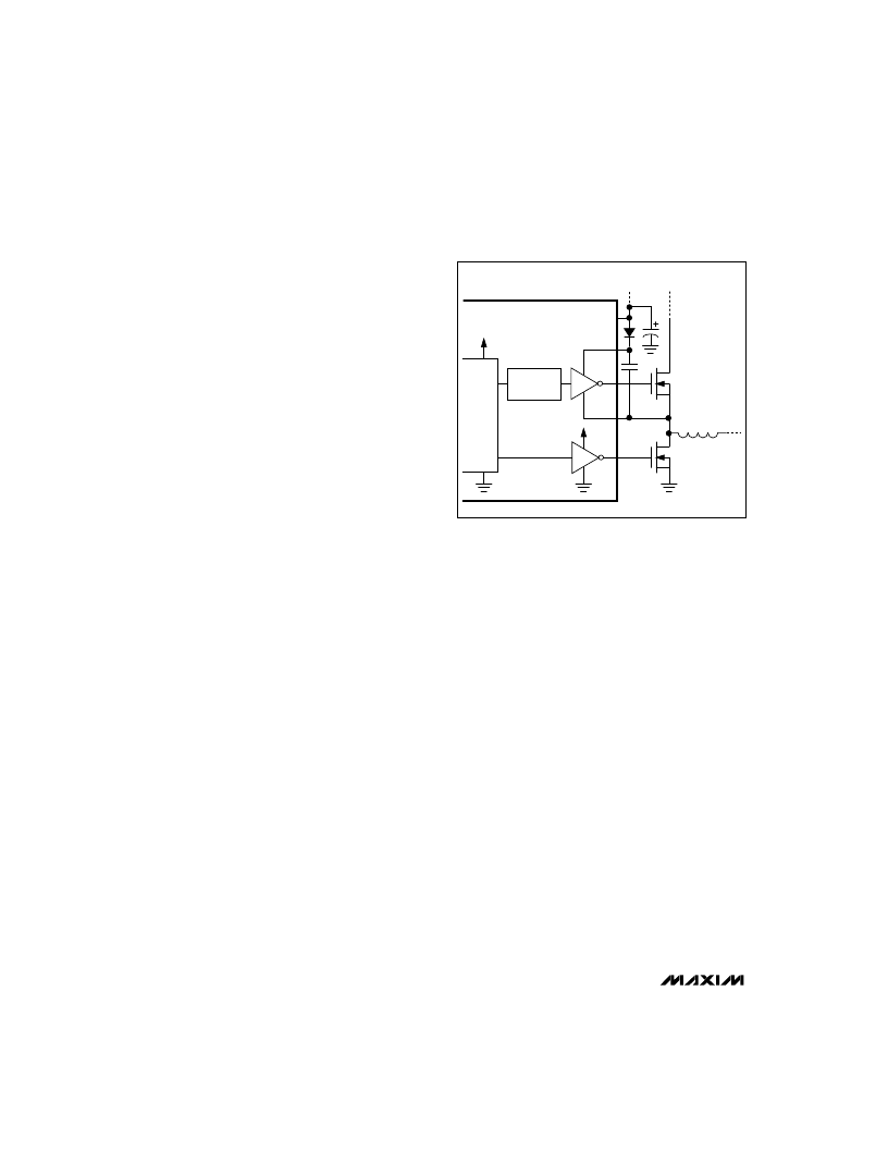
Boost Gate-Driver Supply
Gate-drive voltage for the high-side N-channel switch is
generated with a flying-capacitor boost circuit as shown
in Figure 4. The capacitor is alternately charged from
the VL supply via the diode and placed in parallel with
the high-side MOSFET’s gate-source terminals. On start-
up, the synchronous rectifier (low-side) MOSFET forces
LX_ to 0V and charges the BST_ capacitor to 5V. On the
second half-cycle, the PWM turns on the high-side
MOSFET by connecting the capacitor to the MOSFET
gate by closing an internal switch between BST_ and
DH_. This provides the necessary enhancement voltage
to turn on the high-side switch, an action that “boosts”
the 5V gate-drive signal above the battery voltage.
Ringing seen at the high-side MOSFET gates (DH3 and
DH5) in discontinuous-conduction mode (light loads) is
a natural operating condition caused by the residual
energy in the tank circuit formed by the inductor and
stray capacitance at the LX_ nodes. The gate driver
negative rail is referred to LX_, so any ringing there is
directly coupled to the gate-drive supply.
Modes of Operation
PWM Mode
Under heavy loads—over approximately 25% of full
load—the +3.3V and +5V supplies operate as continu-
ous-current PWM supplies (see Typical Operating
Characteristics). The duty cycle (%ON) is approximately:
%ON = V
OUT
/V
IN
Current flows continuously in the inductor: First, it ramps
up when the power MOSFET conducts; then, it ramps
down during the flyback portion of each cycle as energy
is put into the inductor and then discharged into the load.
Note that the current flowing into the inductor when it is
being charged is also flowing into the load, so the load is
LEVEL
TRANSLATOR
PWM
VL
BST_
DH_
LX_
DL_
VL
BATTERY
INPUT
VL
Figure 4. Boost Supply for Gate Drivers
相關(guān)PDF資料 |
PDF描述 |
|---|---|
| MAX783SEBX | Triple-Output Power-Supply Controller for Notebook Computers |
| MAX783EBX | Hex Inverters 14-CDIP -55 to 125 |
| MAX783RCBX | Triple-Output Power-Supply Controller for Notebook Computers |
| MAX783REBX | Triple-Output Power-Supply Controller for Notebook Computers |
| MAX783SCBX | Triple-Output Power-Supply Controller for Notebook Computers |
相關(guān)代理商/技術(shù)參數(shù) |
參數(shù)描述 |
|---|---|
| MAX783CBX-T | 功能描述:DC/DC 開關(guān)控制器 RoHS:否 制造商:Texas Instruments 輸入電壓:6 V to 100 V 開關(guān)頻率: 輸出電壓:1.215 V to 80 V 輸出電流:3.5 A 輸出端數(shù)量:1 最大工作溫度:+ 125 C 安裝風(fēng)格: 封裝 / 箱體:CPAK |
| MAX783EBX | 功能描述:DC/DC 開關(guān)控制器 RoHS:否 制造商:Texas Instruments 輸入電壓:6 V to 100 V 開關(guān)頻率: 輸出電壓:1.215 V to 80 V 輸出電流:3.5 A 輸出端數(shù)量:1 最大工作溫度:+ 125 C 安裝風(fēng)格: 封裝 / 箱體:CPAK |
| MAX783EBX+ | 功能描述:DC/DC 開關(guān)控制器 RoHS:否 制造商:Texas Instruments 輸入電壓:6 V to 100 V 開關(guān)頻率: 輸出電壓:1.215 V to 80 V 輸出電流:3.5 A 輸出端數(shù)量:1 最大工作溫度:+ 125 C 安裝風(fēng)格: 封裝 / 箱體:CPAK |
| MAX783EBX+T | 功能描述:DC/DC 開關(guān)控制器 RoHS:否 制造商:Texas Instruments 輸入電壓:6 V to 100 V 開關(guān)頻率: 輸出電壓:1.215 V to 80 V 輸出電流:3.5 A 輸出端數(shù)量:1 最大工作溫度:+ 125 C 安裝風(fēng)格: 封裝 / 箱體:CPAK |
| MAX783EBX-T | 功能描述:DC/DC 開關(guān)控制器 RoHS:否 制造商:Texas Instruments 輸入電壓:6 V to 100 V 開關(guān)頻率: 輸出電壓:1.215 V to 80 V 輸出電流:3.5 A 輸出端數(shù)量:1 最大工作溫度:+ 125 C 安裝風(fēng)格: 封裝 / 箱體:CPAK |
發(fā)布緊急采購,3分鐘左右您將得到回復(fù)。