- 您現(xiàn)在的位置:買賣IC網(wǎng) > PDF目錄99963 > 2200SA3F008F24A (GEMS SENSORS CONTROLS) ABSOLUTE, STRAIN GUAGE PRESSURE SENSOR, -15-15Psi, 0.25%, 0-10V, CYLINDRICAL PDF資料下載
參數(shù)資料
| 型號(hào): | 2200SA3F008F24A |
| 廠商: | GEMS SENSORS CONTROLS |
| 元件分類: | Pressure Sensor |
| 英文描述: | ABSOLUTE, STRAIN GUAGE PRESSURE SENSOR, -15-15Psi, 0.25%, 0-10V, CYLINDRICAL |
| 文件頁數(shù): | 2/4頁 |
| 文件大小: | 507K |
| 代理商: | 2200SA3F008F24A |
The Strength of Gems Psibar
Pressure Transducers
Starts with the Science of CVD
Gems Sensors provides the most stable pressure sensor on
the market today by combining advanced sensing technology
with highly automated and revolutionary manufacturing
methods. The result is a sensing element comprised of silicon,
stainless steel, glass, and other metals joined on a molecular
level to form a pressure transducer that is impervious to
aging. If your application requires long life components, Gems
Psibar
transducers are designed with you in mind. Psibar
pressure transducers bring exceptional performance to a wide
variety of applications across multiple industries. The strength
of Psibar
pressure sensors starts with the science of CVD.
Psibar
transducers are manufactured using plasma-enhanced
Chemical Vapor Deposition (CVD) technology. This
sophisticated technique uses a chemical vapor to deposit thin
layers of silicon and silicon dioxide on a stainless steel
substratum to form a very sensitive and accurate polysilicon
strain gauge. Since the elements of the strain gauge are fused
together at the atomic level, the strength and integrity of the
bond far exceeds the adhesives used in common pressure
sensors. Psibar
transducers are inherently more stable and
less sensitive to thermal exposure and pressure cycling than
silicon-based pressure transducers. Your reward is a lower
total cost of ownership.
All sensor conditioning, including amplification, temperature
calibration and filtering is performed by our unique ASIC. It
allows configurable output and pressures ranges, sets the
zero and span tolerance and ensures interchangeability from
unit to unit. The use of an ASIC eliminates laser trimming for
temperature compensation, and unnecessary external
components. Besides reducing size and complexity, the best
reduction our ASIC accomplishes is in the price of a Psibar
transducer.
The CVD sensor and ASIC circuitry is complemented by all
stainless steel construction delivering excellent media
compatibility; all major components are joined by welding.
This construction technique produces a highly stable pressure
transducer that withstands harsh media, and is configurable
to satisfy specific application requirements. Psibar
pressure
transducers are produced in an automated, zero-defect
manufacturing process that incorporates calibration,
configuration and test systems to improve sensor accuracy
and quality. Psibar
pressure transducers deliver exceptionally
superior, long-term performance.
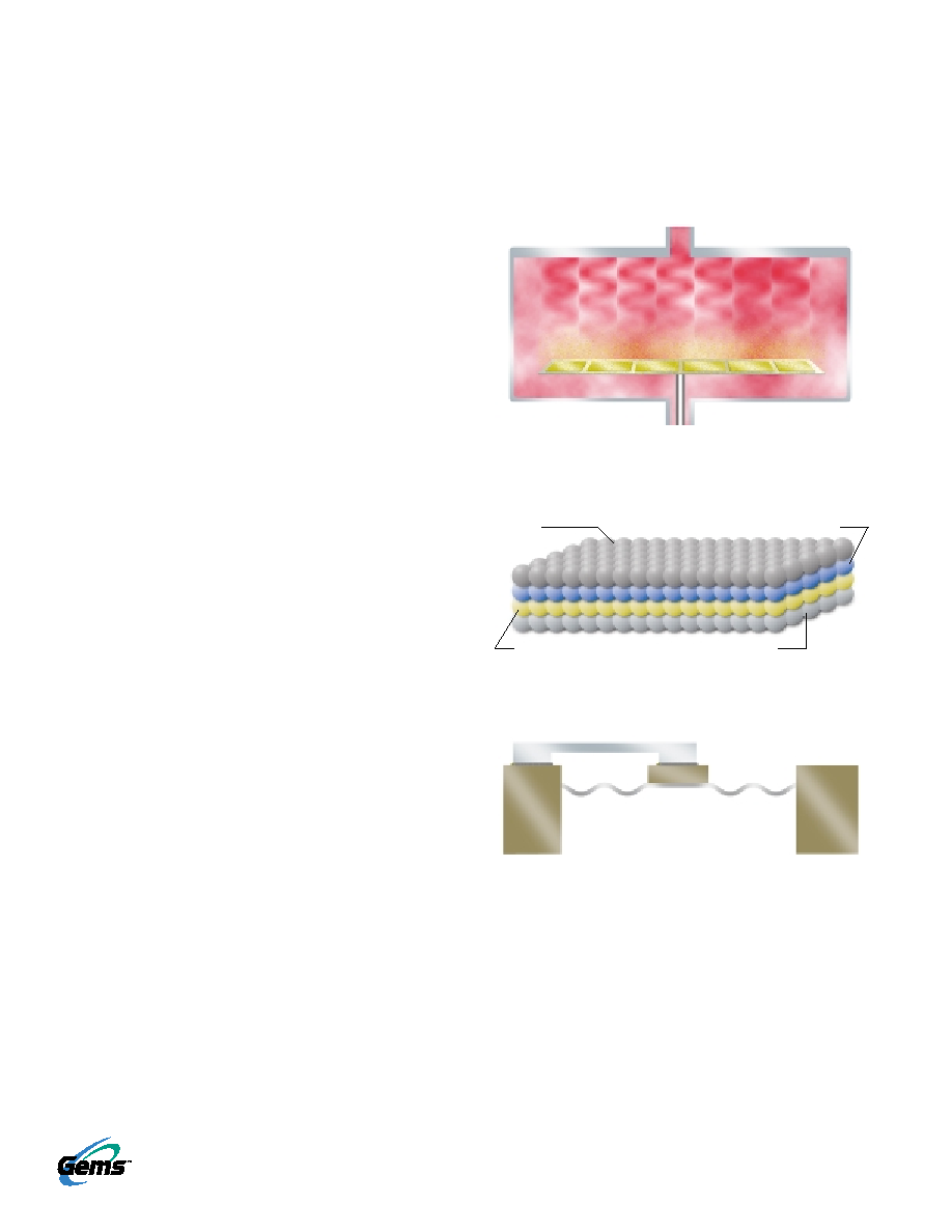
Stainless steel Psibar wafers lie in a gas stream of plasma-enhanced gases. The
PECVD process is used because it deposits high quality silicon at low
temperature, which does not affect the state of the steel gauge. After
deposition, the silicon is ion implanted to modify resistivity.
Call Toll Free 800.378.1600
Advanced sensor manufacturing techniques
allow Psibar sensors to deliver superior
stability and long-life reliability.
The thin film is atomically fused directly to the steel surface of the gauge beam
and therefore follows the shape of the beam very accurately. This atomic fusion
is the foundation for excellent performance and stability.
Cool, Laser Welded
The CVD strain gauge is affixed to the sensor assembly in a precise, automated
laser weld process. A spot weld is made at each end and both sides of the beam
to assure there is no twisting or tilting of the beam while a stitch weld is applied.
Laser welding is fast and cool to prevent any distortion to the strain gauge.
Gas in
Gas out
Titanium
Silicon Dioxide
Polysilicon
Stainless Steel
相關(guān)PDF資料 |
PDF描述 |
|---|---|
| 2200SGH4001224B | GAGE, STRAIN GUAGE PRESSURE SENSOR, 0-4000Psi, 0.15%, 0-10V, CYLINDRICAL |
| 2200SGH4001A24A | GAGE, STRAIN GUAGE PRESSURE SENSOR, 0-4000Psi, 0.25%, 0-10V, CYLINDRICAL |
| 2200SGH4001B3SA | GAGE, STRAIN GUAGE PRESSURE SENSOR, 0-4000Psi, 0.25%, 0-10V, CYLINDRICAL |
| 2200SGH4002A34B | GAGE, STRAIN GUAGE PRESSURE SENSOR, 0-4000Psi, 0.15%, 0-10V, CYLINDRICAL |
| 2200SGH3002B24A | GAGE, STRAIN GUAGE PRESSURE SENSOR, 0-3000Psi, 0.25%, 0-10V, CYLINDRICAL |
相關(guān)代理商/技術(shù)參數(shù) |
參數(shù)描述 |
|---|---|
| 2200SB-10G-A1 | 制造商:SPC Multicomp 功能描述:SOCKET PCB 2 ROW VERT 10WAY 制造商:SPC Multicomp 功能描述:SOCKET, PCB, 2 ROW, VERT, 10WAY 制造商:SPC Multicomp 功能描述:BOARD-BOARD CONN, SOCKET, 10WAY, 2ROW; Series:220SB; Pitch Spacing:1.27mm; No. of Rows:2; No. of Contacts:10; Gender:Receptacle; Contact Termination:Through Hole Vertical; Contact Plating:Gold; Contact Material:Phosphor Bronze ;RoHS Compliant: Yes |
| 2200SB-20G-A1 | 制造商:SPC Multicomp 功能描述:SOCKET PCB 2 ROW VERT 20WAY 制造商:SPC Multicomp 功能描述:SOCKET, PCB, 2 ROW, VERT, 20WAY 制造商:SPC Multicomp 功能描述:BOARD-BOARD CONN, SOCKET, 20WAY, 2ROW; Series:220SB; Pitch Spacing:1.27mm; No. of Rows:2; No. of Contacts:20; Gender:Receptacle; Contact Termination:Through Hole Vertical; Contact Plating:Gold; Contact Material:Phosphor Bronze ;RoHS Compliant: Yes |
| 2200SB-40G-A1 | 制造商:SPC Multicomp 功能描述:SOCKET PCB 2 ROW VERT 40WAY 制造商:SPC Multicomp 功能描述:SOCKET, PCB, 2 ROW, VERT, 40WAY 制造商:PRIVATE LABEL 功能描述:SOCKET, PCB, 2 ROW, VERT, 40WAY, Series:220SB, Pitch Spacing:1.27mm, No. of Rows 制造商:SPC Multicomp 功能描述:BOARD-BOARD CONN, SOCKET, 40WAY, 2ROW, Series:220SB, Pitch Spacing:1.27mm, No. of Rows:2, No. of Contacts:40, Gender:Receptacle, Contact Termination:Through Hole Vertical, Contact Plating:Gold, Contact Material:Phosphor Bronze , RoHS Compliant: Yes |
| 2200SB-50G-A1 | 制造商:SPC Multicomp 功能描述:SOCKET PCB 2 ROW VERT 50WAY 制造商:SPC Multicomp 功能描述:SOCKET, PCB, 2 ROW, VERT, 50WAY 制造商:PRIVATE LABEL 功能描述:SOCKET, PCB, 2 ROW, VERT, 50WAY, Series:220SB, Pitch Spacing:1.27mm, No. of Rows 制造商:SPC Multicomp 功能描述:BOARD-BOARD CONN, SOCKET, 50WAY, 2ROW, Series:220SB, Pitch Spacing:1.27mm, No. of Rows:2, No. of Contacts:50, Gender:Receptacle, Contact Termination:Through Hole Vertical, Contact Plating:Gold, Contact Material:Phosphor Bronze , RoHS Compliant: Yes |
| 2200SB-60G-A1 | 制造商:Keltron 功能描述:2200SB-60G-A1 |
發(fā)布緊急采購,3分鐘左右您將得到回復(fù)。