- 您現(xiàn)在的位置:買賣IC網(wǎng) > PDF目錄384700 > MAX749CSA (MAXIM INTEGRATED PRODUCTS INC) 4-Bit D-type Registers with 3-State Outputs 16-CDIP -55 to 125 PDF資料下載
參數(shù)資料
| 型號: | MAX749CSA |
| 廠商: | MAXIM INTEGRATED PRODUCTS INC |
| 元件分類: | 穩(wěn)壓器 |
| 英文描述: | 4-Bit D-type Registers with 3-State Outputs 16-CDIP -55 to 125 |
| 中文描述: | SWITCHING CONTROLLER, 500 kHz SWITCHING FREQ-MAX, PDSO8 |
| 封裝: | 0.150 INCH, SOP-8 |
| 文件頁數(shù): | 8/12頁 |
| 文件大小: | 105K |
| 代理商: | MAX749CSA |
M
counter rolls over and sets the DAC to -V
OUT(MIN)
,
where -V
OUT(MIN)
= R
FB
x 6.66μA. In other words, a sin-
gle rising edge of ADJ increments the DAC output by
one, and 63 rising edges of ADJ decrement the DAC
output by one.
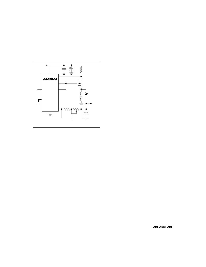
Potentiometer Adjustment
It is also possible to adjust the output voltage using a
potentiometer instead of the internal DAC (Figure 8). On
power-up (V+ applied), the internal current source is set
to mid-scale, or 13.33μA. Choose R1 and R2 with the fol-
lowing equations:
R1 = -V
OUT(MIN)
/13.33μA
R2 = -V
OUT(MAX)
/13.33μA - R1.
Where the potentiometer can be varied from 0 (producing
V
) to R2
(producing V
). Notice that ADJ
is connected to ground, allowing the device to be shut
down.
PWM Adjustment
A positive pulse-width modulated (PWM) logic signal
(e.g., from a microcontroller) can control the MAX749’s
output voltage. Use the PWM signal to pull up the FB
pin through a suitable resistor. An RC network on the
PWM output would also be required. In this configura-
tion, the longer the PWM signal remains high, the more
negative the MAX749’s output will be driven.
Current-S ense Resistor
The current-sense resistor limits the peak switch cur-
rent to 140mV/R
, where R
is the value of the
current-sense resistor, and 140mV is the typical cur-
rent-sense comparator threshold (see V+ to CS Voltage
in the Electrical Characteristics).
To maximize efficiency and reduce the size and cost of
the external components, minimize the peak current.
However, since the output current is a function of the peak
current (Figures 9a-9e), the limit should not be set too low.
No calculations are required to choose the proper cur-
rent-sense resistor; simply follow this two-step procedure:
1. Determine:
- the minimum input voltage, V
- the maximum output voltage, V
OUT(MAX)
, and
- the maximum output current, I
OUT(MAX)
.
For example, assume that the output voltage must be
adjustable to -24V (V
= -24V) at up to 30mA
(I
= 30mA). The supply voltage ranges from
4.75V to 6V (V
IN(MIN)
= 4.75V).
2. In Figures 9a-9e, locate the graph drawn for the
appropriate output voltage (which is either the
desired output voltage or, if that is not shown, the
graph for the nearest voltage more negative than the
desired output). On this graph find the curve for the
highest R
(the lowest current limit) with an out-
put current that is adequate
at the lowest input
voltage.
In this example, select the -24V output graph, Figure 9d.
We then want a curve where I
is
≥
30mA with a 4.75V
input. The 0.3
R
graph shows 25mA of output cur-
rent with a 4.75V input, so we look next at the 0.25
R
SENSE
graph. It shows I
= 30mA for V
= 4.75V and
V
= -24V. Therefore select R
= 0.25
. This pro-
vides a current limit in the range 440mA to 720mA.
Alternatively, a 0.2
sense resistor can be used. This
gives a current limit in the range 550mA to 900mA, but
enables over 40mA to be generated at -24V with input
voltages down to 4.5V. A 0.2
resistor may be easier to
obtain than an 0.25
resistor.
The theoretical design curves shown in Figures 9a-9e
assume the minimum (worst-case) value for the current-
limit comparator threshold. Having selected the cur-
rent-sense resistor, the maximum current limit is given
by 180mV/R
. Use the maximum current-limit fig-
ure when choosing the transistor, coil, and diode.
IRC (see Table 2) makes surface-mount resistors with pre-
ferred values including: 0.1
, 0.2
, 0.3
, 0.5
, and 1.0
.
Digitally Adjustable LCD Bias S upply
8
______________________________________________________________________________________
L1
47
μ
H
DLOW
V
(NEGATIVE)
+4.5V to +6V
INPUT
22
μ
F
0.1
μ
F
CTRL
CS
DHI
R
SENSE
Q1
SMD10P05L
D1
1N5819
22
μ
F
30V
C
COMP
R1
R2
ADJ
MAX749
V+
GND
V
OUT(MIN)
= -R1(13.33
μ
A)
V
OUT(MAX)
= -(R1+R2)(13.33
μ
A)
Figure 8. Using a Potentiometer to Adjust the Output Voltage
相關(guān)PDF資料 |
PDF描述 |
|---|---|
| MAX749EPA | 4-Bit D-type Registers with 3-State Outputs 20-LCCC -55 to 125 |
| MAX749ESA | Digitally Adjustable LCD Bias Supply |
| MAX7524 | Retriggerable Monostable Multivibrators 16-CFP -55 to 125 |
| MAX7624 | CMOS 8-Bit Buffered Multiplying DACs |
| MAX7624CPE | CMOS 8-Bit Buffered Multiplying DACs |
相關(guān)代理商/技術(shù)參數(shù) |
參數(shù)描述 |
|---|---|
| MAX749CSA+ | 功能描述:其他電源管理 Digitally Adjustable LCD Bias Supply RoHS:否 制造商:Texas Instruments 輸出電壓范圍: 輸出電流:4 mA 輸入電壓范圍:3 V to 3.6 V 輸入電流: 功率耗散: 工作溫度范圍:- 40 C to + 110 C 安裝風(fēng)格:SMD/SMT 封裝 / 箱體:VQFN-48 封裝:Reel |
| MAX749CSA+T | 功能描述:顯示驅(qū)動器和控制器 Digitally Adjustable LCD Bias Supply RoHS:否 制造商:Panasonic Electronic Components 工作電源電壓:2.7 V to 5.5 V 最大工作溫度: 安裝風(fēng)格:SMD/SMT 封裝 / 箱體:QFN-44 封裝:Reel |
| MAX749CSA-T | 功能描述:顯示驅(qū)動器和控制器 Digitally Adjustable LCD Bias Supply RoHS:否 制造商:Panasonic Electronic Components 工作電源電壓:2.7 V to 5.5 V 最大工作溫度: 安裝風(fēng)格:SMD/SMT 封裝 / 箱體:QFN-44 封裝:Reel |
| MAX749EPA | 功能描述:顯示驅(qū)動器和控制器 Digitally Adjustable LCD Bias Supply RoHS:否 制造商:Panasonic Electronic Components 工作電源電壓:2.7 V to 5.5 V 最大工作溫度: 安裝風(fēng)格:SMD/SMT 封裝 / 箱體:QFN-44 封裝:Reel |
| MAX749EPA+ | 功能描述:其他電源管理 Digitally Adjustable LCD Bias Supply RoHS:否 制造商:Texas Instruments 輸出電壓范圍: 輸出電流:4 mA 輸入電壓范圍:3 V to 3.6 V 輸入電流: 功率耗散: 工作溫度范圍:- 40 C to + 110 C 安裝風(fēng)格:SMD/SMT 封裝 / 箱體:VQFN-48 封裝:Reel |
發(fā)布緊急采購,3分鐘左右您將得到回復(fù)。