- 您現(xiàn)在的位置:買賣IC網(wǎng) > PDF目錄384700 > MAX747ESD (MAXIM INTEGRATED PRODUCTS INC) Parallel-Load 8-Bit Shift Registers 16-CFP -55 to 125 PDF資料下載
參數(shù)資料
| 型號: | MAX747ESD |
| 廠商: | MAXIM INTEGRATED PRODUCTS INC |
| 元件分類: | 穩(wěn)壓器 |
| 英文描述: | Parallel-Load 8-Bit Shift Registers 16-CFP -55 to 125 |
| 中文描述: | SWITCHING CONTROLLER, 100 kHz SWITCHING FREQ-MAX, PDSO14 |
| 封裝: | 0.150 INCH, PLASTIC, SO-14 |
| 文件頁數(shù): | 11/12頁 |
| 文件大小: | 136K |
| 代理商: | MAX747ESD |
M
High-Effic ienc y PWM, S tep-Down
P-Channel DC-DC Controller
______________________________________________________________________________________
11
S etting the Low-Battery Detec tor V oltage
Select R1 between 10k
and 1M
.
Connect a pull-up resistor (e.g., 100k
) between LBO
and V
OUT
(Figure 4).
__________Applic ations Information
Layout Considerations
Due to high current levels and fast switching
waveforms, which radiate noise, proper MAX747 PC
board layout is essential. Protect sensitive analog
grounds by using a star ground configuration. Use an
adequate ground plane and minimize ground noise by
connecting GND, the anode of the steering Schottky
diode, the input bypass capacitor ground lead, and the
output filter capacitor ground lead to a single point
(star ground configuration). Also, minimize lead lengths
to minimize stray capacitance, trace resistance, and
radiated noise. Place bypass capacitor C3 as close as
possible to V+ and GND.
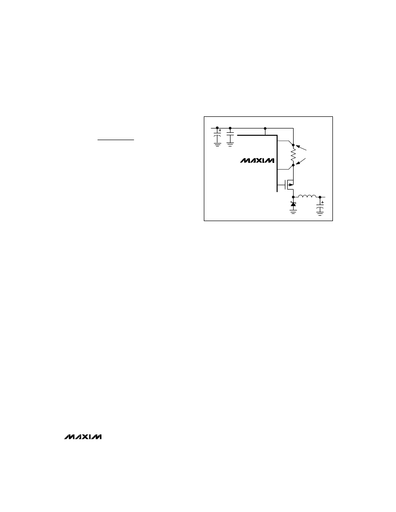
AV+ and CS are the inputs to the differential-input
current-sense amplifier. Use a Kelvin connection
across the sense resistor as shown in Figure 6. Note
that even though AV+ also functions as the supply
voltage for sensitive analog circuitry, a separate AV+
bypass capacitor should not be used. By not using a
capacitor, any noise appearing at the CS input will also
appear at the AV+ input and will appear as a common-
mode signal to the current-sense amplifier. A separate
AV+ capacitor causes the noise to appear only on one
input, and this differential noise will be amplified,
adversely affecting circuit operation.
Similarly, CC (or FB in adjustable-output operation) is a
sensitive input that should not be shorted to any node.
Avoid shorting CC when probing the circuit, as this
may damage the device.
S witc hing Waveforms
A region exists between CCM and DCM where the
inductor current operates in both modes, as shown in
the Idle-Mode Moderate current EXT waveform in the
Typical Operating Characteristics. As the output
voltage varies, it is fed back into CC and the duty cycle
is adjusted to compensate for this change. The switch
is considered off when V
≤
the P-FET’s V
threshold voltage. Once the switch is off, the voltage at
EXT is pulled to V+ and the P-FET drain voltage is a
Schottky diode drop below GND. However, in this “in-
between” mode (due to the changing duty cycle
inherent with DCM), when the device is at maximum
duty cycle, EXT turns off at V+ - V
GS
. But it is not
always pulled to V+ because the switch sometimes
turns on again after a minimum off-time before EXT can
be pulled to V+. The result is short spikes that appear
on the EXT waveform in the Typical Operating
Characteristics.
AC S tability with Low
Input/Output Differentials
At low input/output differentials, the inductor current
cannot slew quickly to respond to load changes, so the
output filter capacitor must hold up the voltage as the
load transient is applied. In Figure 1a’s circuit, for
V+ = 6.5V, increase the output filter capacitor to 700μF
(Sprague 595D low-ESR capacitors) to obtain a
transient response less than 250mV with a load step
from 200mA to 2.5A. For V+ = 6V and V
= 5V,
increase the output filter capacitor to approximately
1000μF. As V+ increases, the device will no longer be
operating near full duty cycle with light loads, allowing
it to adjust to full duty cycle when the load transient is
applied and, in turn, allowing smaller output filter
capacitors to be used.
Dual-Mode Operation
The MAX747 is designed in either fixed-output mode
(5V-output, FB = GND) or in adjustable mode (FB = 2V)
using a resistor divider. It is not designed to be
switched from one mode to another when powered up;
however, in adjustment mode, switching between two
different resistor dividers is acceptable.
R2
R1 (V
V
V
TRIP
REF
REF
=
)
AV+
MAX747
V
IN
CS
RSENSE
P
EXT
L1
V
OUT
KELVIN SENSE
CONNECTION
V+
Figure 6. Kelvin Connection for Current-Sense Amplifier
相關(guān)PDF資料 |
PDF描述 |
|---|---|
| MAX747MJD | Parallel-Load 8-Bit Shift Registers 16-CDIP -55 to 125 |
| MAX7480 | Parallel-Load 8-Bit Shift Registers 20-LCCC -55 to 125 |
| MAX7480EPA | Parallel-Load 8-Bit Shift Registers 16-CDIP -55 to 125 |
| MAX7480ESA | Parallel-Load 8-Bit Shift Registers 16-CFP -55 to 125 |
| MAX748A | Synchronous 4-Bit Up/Down Binary Counters 20-LCCC -55 to 125 |
相關(guān)代理商/技術(shù)參數(shù) |
參數(shù)描述 |
|---|---|
| MAX747ESD+ | 功能描述:DC/DC 開關(guān)控制器 Integrated Circuits (ICs) RoHS:否 制造商:Texas Instruments 輸入電壓:6 V to 100 V 開關(guān)頻率: 輸出電壓:1.215 V to 80 V 輸出電流:3.5 A 輸出端數(shù)量:1 最大工作溫度:+ 125 C 安裝風(fēng)格: 封裝 / 箱體:CPAK |
| MAX747ESD+T | 功能描述:DC/DC 開關(guān)控制器 Integrated Circuits (ICs) RoHS:否 制造商:Texas Instruments 輸入電壓:6 V to 100 V 開關(guān)頻率: 輸出電壓:1.215 V to 80 V 輸出電流:3.5 A 輸出端數(shù)量:1 最大工作溫度:+ 125 C 安裝風(fēng)格: 封裝 / 箱體:CPAK |
| MAX747ESD-T | 功能描述:DC/DC 開關(guān)控制器 RoHS:否 制造商:Texas Instruments 輸入電壓:6 V to 100 V 開關(guān)頻率: 輸出電壓:1.215 V to 80 V 輸出電流:3.5 A 輸出端數(shù)量:1 最大工作溫度:+ 125 C 安裝風(fēng)格: 封裝 / 箱體:CPAK |
| MAX747EVKIT-SO | 功能描述:DC/DC 開關(guān)控制器 RoHS:否 制造商:Texas Instruments 輸入電壓:6 V to 100 V 開關(guān)頻率: 輸出電壓:1.215 V to 80 V 輸出電流:3.5 A 輸出端數(shù)量:1 最大工作溫度:+ 125 C 安裝風(fēng)格: 封裝 / 箱體:CPAK |
| MAX747MJD | 功能描述:DC/DC 開關(guān)控制器 RoHS:否 制造商:Texas Instruments 輸入電壓:6 V to 100 V 開關(guān)頻率: 輸出電壓:1.215 V to 80 V 輸出電流:3.5 A 輸出端數(shù)量:1 最大工作溫度:+ 125 C 安裝風(fēng)格: 封裝 / 箱體:CPAK |
發(fā)布緊急采購,3分鐘左右您將得到回復(fù)。