- 您現(xiàn)在的位置:買賣IC網(wǎng) > PDF目錄385549 > MAX7432 (Maxim Integrated Products, Inc.) Quadruple 2-Line To 1-Line Data Selectors/Multiplexers 20-LCCC -55 to 125 PDF資料下載
參數(shù)資料
| 型號(hào): | MAX7432 |
| 廠商: | Maxim Integrated Products, Inc. |
| 英文描述: | Quadruple 2-Line To 1-Line Data Selectors/Multiplexers 20-LCCC -55 to 125 |
| 中文描述: | 標(biāo)準(zhǔn)清晰度、視頻重建濾波器及緩沖器 |
| 文件頁(yè)數(shù): | 10/21頁(yè) |
| 文件大?。?/td> | 444K |
| 代理商: | MAX7432 |
第1頁(yè)第2頁(yè)第3頁(yè)第4頁(yè)第5頁(yè)第6頁(yè)第7頁(yè)第8頁(yè)第9頁(yè)當(dāng)前第10頁(yè)第11頁(yè)第12頁(yè)第13頁(yè)第14頁(yè)第15頁(yè)第16頁(yè)第17頁(yè)第18頁(yè)第19頁(yè)第20頁(yè)第21頁(yè)

M
Standard Definition Video Reconstruction
Filters and Buffers
10
______________________________________________________________________________________
CLEVEL:
Clamp Level bit. A logic 0 selects a clamp
level of 1V while a logic 0 selects a clamp level of 1.5V
at the output.
[BOOST1, BOOST0]:
High-Frequency Boost Control bits.
The adjust bits select the amount of high-frequency boost
for the filter. Table 2 defines four levels of adjustment.
OUTDISABLE:
Output Disable bit. A logic 0 selects
normal operation while a logic 1 places the output in a
high-impedance state.
MAX7430 Control Register
Table 3 defines the structure of the MAX7430 16-bit con-
trol register programmed by MSPB. This register controls
the selection of IN_A or IN_B, selection of filter 1 or 2, filter
bypassing, clamp-level selection, high-frequency boost
control, and output disable. See
Maxim
’
s Single Pin Bus
Interface (MSPB)
section for detailed programming
instructions.
ABSEL_:
Channel Select bit. A logic zero selects the
input at IN_B to be processed while a logic 1 selects
the input at IN_A to be processed.
BYPASS_:
Filter Bypass Select bit. A logic 1 selects
the channel filter while a logic 0 bypasses the channel
filter.
CLEVEL_:
Clamp Level bit. A logic 0 selects a channel
clamp level of 1V while a logic 0 selects a channel
clamp level of 1.5V at the output.
[BOOST1_, BOOST0_]:
High-Frequency Boost Control
bits. The adjust bits select the amount of high-frequency
boost for the channel filter. Table 4 defines four levels of
adjustment.
OUTDISABLE_:
Output Disable bit. A logic 0 selects
normal channel output operation while a logic 1 puts
the channel output in a high-impedance state.
MAX7432 Control Register
Table 5 defines the structure of the MAX7432 24-bit
control register programmed by MSPB. This register
controls the selection of IN_A or IN_B, selection of filter
1, 2, or 3, filter bypassing, clamp-level selection, high-
frequency boost control, and output disable. See
Maxim
’
s Single Pin Bus Interface (MSPB)
section for
detailed programming instructions.
ABSEL_:
Channel Select bit. A logic zero selects the
input at IN_B to be processed while a logic 1 selects
the input at IN_A to be processed.
BYPASS_:
Filter Bypass Select bit. A logic 1 selects
the channel filter while a logic 0 bypasses the channel
filter.
CLEVEL_:
Clamp Level bit. A logic 0 selects a channel
clamp level of 1V while a logic 0 selects a channel
clamp level of 1.5V at the output.
[BOOST1_, BOOST0_]:
High-Frequency Boost Control
bits. The adjust bits select the amount of high-frequency
boost for the channel filter. Table 6 defines four levels of
adjustment.
OUTDISABLE_:
Output Disable Bit. A logic 0 selects
normal channel output operation while a logic 1 puts
the channel output in high-impedance state.
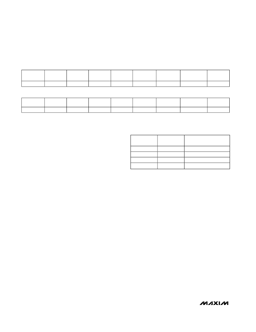
(MSB)
NAME
—
ABSEL2
BYPASS2
CLEVEL2
BOOST1(2)
BOOST0(2)
OUT
DISABLE2
—
DEFAULT
0
1
1
0
0
0
0
0
NAME
—
ABSEL1
BYPASS1
CLEVEL1
BOOST1(1)
BOOST0(1)
OUT
DISABLE1
0
—
DEFAULT
0
1
1
0
0
0
0
FIRST BIT
(LSB)
Table 3. MAX7430 Control Register
BOOST1_
BOOST0_
RELATIVE HIGH-
FREQUENCY BOOST
0
0
1
1
0
1
0
1
0
0.45dB
0.90dB
1.35dB
Table 4. Boost Level Programming
相關(guān)PDF資料 |
PDF描述 |
|---|---|
| MAX7432EUD | Quadruple 2-Line To 1-Line Data Selectors/Multiplexers 16-CDIP -55 to 125 |
| MAX7428EKA-T | Standard Definition Video Reconstruction Filters and Buffers |
| MAX743CWE | Dual-Output, Switch-Mode Regulator(+5V to +-15V or +-12V) |
| MAX743CPE | Quadruple 2-Line To 1-Line Data Selectors/Multiplexers 16-CFP -55 to 125 |
| MAX743EPE | Dual-Output, Switch-Mode Regulator(+5V to +-15V or +-12V) |
相關(guān)代理商/技術(shù)參數(shù) |
參數(shù)描述 |
|---|---|
| MAX7432AEUD | 制造商:Rochester Electronics LLC 功能描述: 制造商:Maxim Integrated Products 功能描述: |
| MAX7432AEUD+ | 制造商:Rochester Electronics LLC 功能描述: 制造商:Maxim Integrated Products 功能描述: |
| MAX7432EUD | 功能描述:有源濾波器 RoHS:否 制造商:Maxim Integrated 通道數(shù)量:1 截止頻率:150 KHz 電源電壓-最大:11 V 電源電壓-最小:4.74 V 最大工作溫度:+ 85 C 安裝風(fēng)格:Through Hole 封裝 / 箱體:PDIP N 封裝:Tube |
| MAX7432EUD/GG8 | 功能描述:有源濾波器 RoHS:否 制造商:Maxim Integrated 通道數(shù)量:1 截止頻率:150 KHz 電源電壓-最大:11 V 電源電壓-最小:4.74 V 最大工作溫度:+ 85 C 安裝風(fēng)格:Through Hole 封裝 / 箱體:PDIP N 封裝:Tube |
| MAX7432EUD+ | 功能描述:視頻 IC Standard Def Video Reconstruction Filtr RoHS:否 制造商:Fairchild Semiconductor 工作電源電壓:5 V 電源電流:80 mA 最大工作溫度:+ 85 C 封裝 / 箱體:TSSOP-28 封裝:Reel |
發(fā)布緊急采購(gòu),3分鐘左右您將得到回復(fù)。