- 您現(xiàn)在的位置:買賣IC網(wǎng) > PDF目錄383453 > MAX653MJA (MAXIM INTEGRATED PRODUCTS INC) 5V/3.3V/3V/Adjustable, High-Efficiency, Low IQ, Step-Down DC-DC Converters PDF資料下載
參數(shù)資料
| 型號(hào): | MAX653MJA |
| 廠商: | MAXIM INTEGRATED PRODUCTS INC |
| 元件分類: | 穩(wěn)壓器 |
| 英文描述: | 5V/3.3V/3V/Adjustable, High-Efficiency, Low IQ, Step-Down DC-DC Converters |
| 中文描述: | 1 A SWITCHING REGULATOR, CDIP8 |
| 封裝: | CERAMIC, DIP-8 |
| 文件頁數(shù): | 2/12頁 |
| 文件大?。?/td> | 166K |
| 代理商: | MAX653MJA |
M
5V /3.3V /3V /Adjustable, High-Effic ienc y,
Low I
Q
, S tep-Down DC-DC Converters
2
_______________________________________________________________________________________
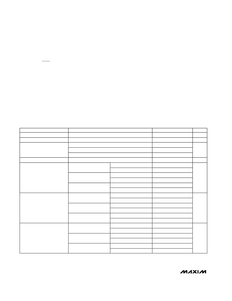
ABSOLUTE MAXIMUM RATINGS
V+...........................................................................................12V
LX .........................................................(V+ - 12V) to (V+ + 0.3V)
LBI, LBO, VFB, SHDN, VOUT........................-0.3V to (V+ + 0.3V)
LX Output Current (Note 1)......................................................1A
LBO Output Current............................................................10mA
Continuous Power Dissipation (T
A
= +70°C)
Plastic DIP (derate 9.09mW/°C above +70°C) .............727mW
SO (derate 5.88mW/°C above +70°C)..........................471mW
CERDIP (derate 8.00mW/°C above +70°C)..................640mW
ELECTRICAL CHARACTERISTICS
(V+ = 9V for the MAX639, V+ = 5V for the MAX640/MAX653, I
LOAD
= 0mA, T
A
= T
MIN
to T
MAX
, typical values are at T
A
= +25°C,
unless otherwise noted.)
Stresses beyond those listed under “Absolute Maximum Ratings” may cause permanent damage to the device. These are stress ratings only, and functional
operation of the device at these or any other conditions beyond those indicated in the operational sections of the specifications is not implied. Exposure to
absolute maximum rating conditions for extended periods may affect device reliability.
PARAMETER
MIN
4.0
TYP
MAX
11.5
20
5.20
UNITS
V
μA
91
94
87
91
85
89
12.5
16.7
8.8
71.4
8.3
Dropout Voltage
0.5
V
Output Voltage (Note 2)
2.88
3.00
3.12
V
3.17
3.30
3.43
Supply Current
Supply Voltage
10
5.00
4.80
Efficiency
%
CONDITIONS
MAX653
I
OUT
= 100mA, L = 100μH
MAX653, V+ = 4.0V to 11.5V, 0mA < I
OUT
< 100mA
MAX640, V+ = 4.0V to 11.5V, 0mA < I
OUT
< 100mA
MAX639
MAX640
SHDN
= V+, no load
MAX639, V+ = 6.0V to 11.5V, 0mA < I
OUT
< 100mA
Operating Temperature Ranges:
MAX639C_ _ .......................................................0°C to +70°C
MAX639E_ _ ....................................................-40°C to +85°C
MAX639MJ A ..................................................-55°C to +125°C
Storage Temperature Range.............................-65°C to +160°C
Lead Temperature (soldering, 10sec) .............................+300°C
I
OUT
= 100mA, L = 100μH
I
OUT
= 25mA, L = 470μH
I
OUT
= 100mA, L = 100μH
I
OUT
= 25mA, L = 470μH
I
OUT
= 100mA, L = 100μH
I
OUT
= 25mA, L = 470μH
V+ = 9V, V
OUT
= 5V
V+ = 6V, V
OUT
= 3V
V+ = 9V, V
OUT
= 3.3V
V+ = 4V, V
OUT
= 3.3V
V+ = 9V, V
OUT
= 3V
V+ = 4V, V
OUT
= 3V
V+ = 9V, V
OUT
= 5V
V+ = 6V, V
OUT
= 3V
V+ = 9V, V
OUT
= 3.3V
V+ = 4V, V
OUT
= 3.3V
V+ = 9V, V
OUT
= 3V
V+ = 4V, V
OUT
= 3V
Switch On-Time
42.5
9.0
16.6
13.3
13.3
14.6
50.0
11.7
19.5
15.6
15.6
17.2
57.5
13.5
22.4
17.9
17.9
19.8
μs
10.6
14.2
7.5
60.7
7.1
14.4
19.2
10.1
82.1
9.5
MAX653
MAX639
MAX640
Switch Off-Time
14.6
17.2
19.8
μs
MAX653
MAX639
MAX640
Note 1:
Peak inductor current must be limited to 600mA by using an inductor of 100μH or greater.
相關(guān)PDF資料 |
PDF描述 |
|---|---|
| MAX639ESA | 5V/3.3V/3V/Adjustable, High-Efficiency, Low IQ, Step-Down DC-DC Converters |
| MAX639MJA | 5V/3.3V/3V/Adjustable, High-Efficiency, Low IQ, Step-Down DC-DC Converters |
| MAX641XEPA | RADIATION HARDENED HIGH EFFICIENCY, 5 AMP SWITCHING REGULATORS |
| MAX642 | 30 AMP MINIATURE POWER RELAY |
| MAX643 | 30 AMP MINIATURE POWER RELAY |
相關(guān)代理商/技術(shù)參數(shù) |
參數(shù)描述 |
|---|---|
| MAX654CPD | 制造商:Maxim Integrated Products 功能描述:CONTACT FACTORY - Rail/Tube |
| MAX654CSD | 制造商:Maxim Integrated Products 功能描述: |
| MAX654CSD-T | 制造商:Rochester Electronics LLC 功能描述: 制造商:Maxim Integrated Products 功能描述: |
| MAX654ESD | 制造商:Rochester Electronics LLC 功能描述: 制造商:Maxim Integrated Products 功能描述: |
| MAX655CSD | 制造商:Rochester Electronics LLC 功能描述: 制造商:Maxim Integrated Products 功能描述: |
發(fā)布緊急采購,3分鐘左右您將得到回復(fù)。