- 您現(xiàn)在的位置:買賣IC網(wǎng) > PDF目錄383427 > MAX5075AAUA (MAXIM INTEGRATED PRODUCTS INC) Push-Pull FET Driver with Integrated Oscillator and Clock Output PDF資料下載
參數(shù)資料
| 型號(hào): | MAX5075AAUA |
| 廠商: | MAXIM INTEGRATED PRODUCTS INC |
| 元件分類: | MOSFETs |
| 英文描述: | Push-Pull FET Driver with Integrated Oscillator and Clock Output |
| 中文描述: | 3 A HALF BRDG BASED MOSFET DRIVER, PDSO8 |
| 封裝: | MO-187, MSOP-8 |
| 文件頁數(shù): | 7/8頁 |
| 文件大小: | 234K |
| 代理商: | MAX5075AAUA |
Power Dissipation
The power dissipation of the MAX5075 is a function of
the sum of the quiescent current and the output current
(either capacitive or resistive load). Maintain the sum of
the currents so the maximum power dissipation limit is
not exceeded. The power dissipation (P
DISS
) due to the
quiescent switching supply current (I
CCSW
) can be cal-
culated as:
P
DISS
= V
CC
x I
CCSW
For capacitive loads, use the following equation to esti-
mate the power dissipation:
P
LOAD
= 2 x C
LOAD
x V
CC
2
x f
NDRV_
where C
LOAD
is the capacitive load at NDRV1 and
NDRV2, V
CC
is the supply voltage, and f
NDRV_
is the
MAX5075 NDRV_ switching frequency.
Calculate the total power dissipation (P
T
) as follows:
P
T
= P
DISS
+ P
LOAD
Layout Recommendations
The MAX5075 sources and sinks large currents that can
create very fast rise and fall edges at the gate of the
switching MOSFETs. The high di/dt can cause unaccept-
able ringing if the trace lengths and impedances are not
well controlled. Use the following PC board layout guide-
lines when designing with the MAX5075:
Place one or more 0.1μF decoupling ceramic
capacitors from V
CC
to PGND as close to the
device as possible. Connect V
CC
and all ground
pins to large copper areas. Place one bulk capaci-
tor of 10μF on the PC board with a low-impedance
path to the V
CC
input and PGND of the MAX5075.
Two AC current loops form between the device and
the gate of the driven MOSFETs. The MOSFETs
look like a large capacitance from gate to source
when the gate pulls low. The current loop is from
the MOSFET gate to NDRV1 and NDRV2 of the
MAX5075, to PGND, and to the source of the
MOSFET. When the gate of the MOSFET pulls high,
the current is from the V
CC
terminal of the decou-
pling capacitor, to V
CC
of the MAX5075, to NDRV1
and NDRV2, and to the MOSFET gate and source.
Both charging current and discharging current loops
are important. Minimize the physical distance and
the impedance in these AC current paths.
Keep the device as close to the MOSFET as possible.
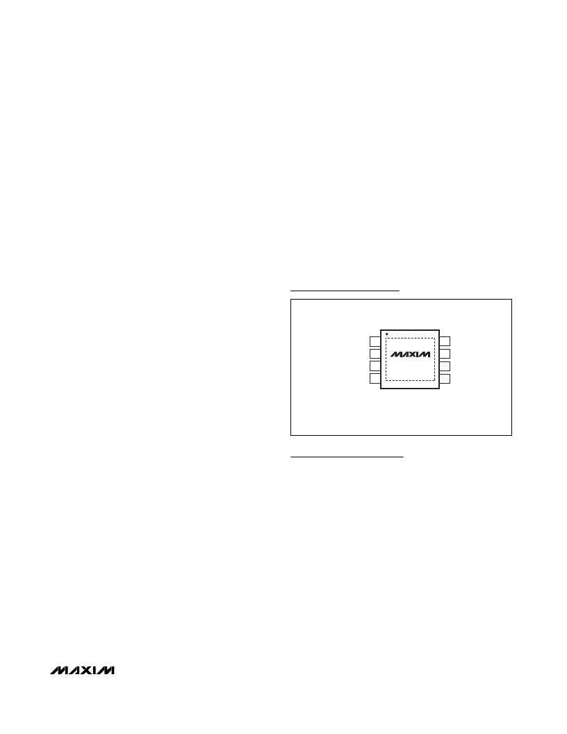
Chip Information
TRANSISTOR COUNT: 1335
PROCESS: BiCMOS
M
Push-Pull FET Driver with Integrated Oscillator
and Clock Output
_______________________________________________________________________________________
7
1
2
3
4
8
7
6
5
V
CC
NDRV2
NDRV1
PGND
DGND
RT
I.C.
CLK
*EP
*EXPOSED PADDLE CONNECTED TO DGND.
MAX5075
μ
MAX
TOP VIEW
Pin Configuration
相關(guān)PDF資料 |
PDF描述 |
|---|---|
| MAX5075B | Push-Pull FET Driver with Integrated Oscillator and Clock Output |
| MAX5075BAUA | Push-Pull FET Driver with Integrated Oscillator and Clock Output |
| MAX5075C | Push-Pull FET Driver with Integrated Oscillator and Clock Output |
| MAX5075CAUA | Push-Pull FET Driver with Integrated Oscillator and Clock Output |
| MAX507AMRG | Voltage-Output, 12-Bit DACs with Internal Reference |
相關(guān)代理商/技術(shù)參數(shù) |
參數(shù)描述 |
|---|---|
| MAX5075AAUA+ | 功能描述:功率驅(qū)動(dòng)器IC Push-Pull FET Driver w/Osc & Clock RoHS:否 制造商:Micrel 產(chǎn)品:MOSFET Gate Drivers 類型:Low Cost High or Low Side MOSFET Driver 上升時(shí)間: 下降時(shí)間: 電源電壓-最大:30 V 電源電壓-最小:2.75 V 電源電流: 最大功率耗散: 最大工作溫度:+ 85 C 安裝風(fēng)格:SMD/SMT 封裝 / 箱體:SOIC-8 封裝:Tube |
| MAX5075AAUA+T | 功能描述:功率驅(qū)動(dòng)器IC Push-Pull FET Driver w/Osc & Clock RoHS:否 制造商:Micrel 產(chǎn)品:MOSFET Gate Drivers 類型:Low Cost High or Low Side MOSFET Driver 上升時(shí)間: 下降時(shí)間: 電源電壓-最大:30 V 電源電壓-最小:2.75 V 電源電流: 最大功率耗散: 最大工作溫度:+ 85 C 安裝風(fēng)格:SMD/SMT 封裝 / 箱體:SOIC-8 封裝:Tube |
| MAX5075AAUA-T | 功能描述:功率驅(qū)動(dòng)器IC Push-Pull FET Driver w/Osc & Clock RoHS:否 制造商:Micrel 產(chǎn)品:MOSFET Gate Drivers 類型:Low Cost High or Low Side MOSFET Driver 上升時(shí)間: 下降時(shí)間: 電源電壓-最大:30 V 電源電壓-最小:2.75 V 電源電流: 最大功率耗散: 最大工作溫度:+ 85 C 安裝風(fēng)格:SMD/SMT 封裝 / 箱體:SOIC-8 封裝:Tube |
| MAX5075B | 制造商:MAXIM 制造商全稱:Maxim Integrated Products 功能描述:Push-Pull FET Driver with Integrated Oscillator and Clock Output |
| MAX5075BAUA | 功能描述:功率驅(qū)動(dòng)器IC Push-Pull FET Driver w/Osc & Clock RoHS:否 制造商:Micrel 產(chǎn)品:MOSFET Gate Drivers 類型:Low Cost High or Low Side MOSFET Driver 上升時(shí)間: 下降時(shí)間: 電源電壓-最大:30 V 電源電壓-最小:2.75 V 電源電流: 最大功率耗散: 最大工作溫度:+ 85 C 安裝風(fēng)格:SMD/SMT 封裝 / 箱體:SOIC-8 封裝:Tube |
發(fā)布緊急采購(gòu),3分鐘左右您將得到回復(fù)。