- 您現(xiàn)在的位置:買賣IC網(wǎng) > PDF目錄383420 > MAX477EVKIT (Maxim Integrated Products, Inc.) Low-Power.Adjustable-Output.Positive-Voltage Linear Regulator[ICL7663/ICL7663AC/D/ICL7663ACPA/ICL7663ACSA/ICL7663ACSA-T/ICL7663AEPA/ICL7663AESA/ICL7663AESA-T/ICL7663AIJA/ICL7663AITV-4/ICL7663BCPA/ICL7663BCSA/ICL7663BITV/ICL7663C/D/ICL7663CPA/ICL7663CSA/ICL7663CSA-T/ICL7663CTV/ICL7663EJA/ICL7663EPA/ICL7663ESA/ICL7663ESA-T/ICL7663IJA/ICL7663IPA/ICL7663ISA] PDF資料下載
參數(shù)資料
| 型號: | MAX477EVKIT |
| 廠商: | Maxim Integrated Products, Inc. |
| 英文描述: | Low-Power.Adjustable-Output.Positive-Voltage Linear Regulator[ICL7663/ICL7663AC/D/ICL7663ACPA/ICL7663ACSA/ICL7663ACSA-T/ICL7663AEPA/ICL7663AESA/ICL7663AESA-T/ICL7663AIJA/ICL7663AITV-4/ICL7663BCPA/ICL7663BCSA/ICL7663BITV/ICL7663C/D/ICL7663CPA/ICL7663CSA/ICL7663CSA-T/ICL7663CTV/ICL7663EJA/ICL7663EPA/ICL7663ESA/ICL7663ESA-T/ICL7663IJA/ICL7663IPA/ICL7663ISA] |
| 中文描述: | 低Power.Adjustable - Output.Positive電壓線性穩(wěn)壓器[ICL7663/ICL7663AC/D/ICL7663ACPA/ICL7663ACSA/ICL7663ACSA-T/ICL7663AEPA/ICL7663AESA/ICL7663AESA-T/ICL7663AIJA/ICL7663AITV-4/ICL7663BCPA/ICL7663BCSA/ICL7663BITV/ICL7663C / D/ICL7663CPA/ICL7663CSA/ICL7663CSA-T/ICL7663CTV/ICL7663EJA/ICL7663EPA/ICL7663ESA/ICL7663ESA-T/ICL7663IJA/ICL7663IPA/ICL7663ISA] |
| 文件頁數(shù): | 8/12頁 |
| 文件大小: | 318K |
| 代理商: | MAX477EVKIT |
M
Power-Supply Sequencing and
Overvoltage Protection
CAUTION: Do not exceed the absolute maximum
ratings. Stresses beyond the listed ratings can
cause permanent damage to the devices.
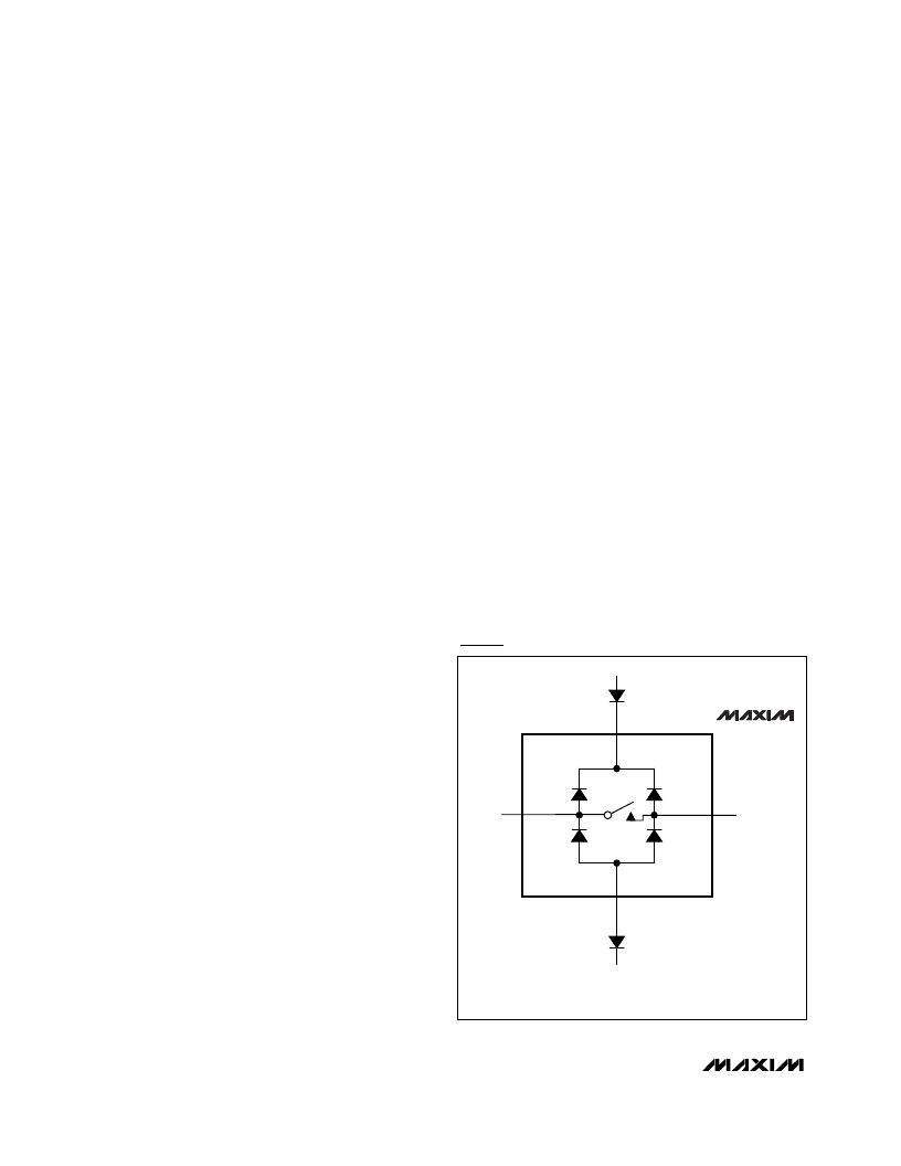
Proper power-supply sequencing is recommended for
all CMOS devices. Always apply V+ before applying
analog signals, especially if the analog signal is not
current limited. If this sequencing is not possible, and if
the analog inputs are not current limited to <20mA, add
a small-signal diode, D1, as shown in Figure 1. If the
analog signal can dip below GND, add D2. Adding
protection diodes reduces the analog signal range to a
diode drop (about 0.7V) below V+ (for D1), and to a
diode drop above ground (for D2). Leakage is unaffect-
ed by adding the diodes. On-resistance increases
slightly at low supply voltages. Maximum supply volt-
age (V+) must not exceed +11V.
Adding protection diodes causes the logic thresholds to
be shifted relative to the power-supply rails. The most
significant shift occurs when using low supply voltages
(+5V or less). With a +5V supply, TTL compatibility is
not guaranteed when protection diodes are added.
Driving IN1 and IN2 all the way to the supply rails (i.e.,
to a diode drop higher than the V+ pin, or to a diode
drop lower than the GND pin) is always acceptable.
Protection diodes D1 and D2 also protect against some
overvoltage situations. Using the circuit in Figure 1, no
damage results if the supply voltage is below the
absolute maximum rating (+12V) and if a fault voltage
up to the absolute maximum rating (V+ + 0.3V) is
applied to an analog signal terminal.
UCSP Package Consideration
For general UCSP package information and PC layout
considerations, please refer to the Maxim Application
Note,
“
Wafer-Level Chip-Scale Packages.
”
UCSP Reliability
The chip-scale package (UCSP) represents a unique
package that greatly reduces board space compared
to other packages. UCSP reliability is integrally linked
to the user
’
s assembly methods, circuit board material,
and usage environment. The user should closely review
these areas when considering a UCSP. Performance
through Operation Life Test and Moisture Resistance is
equal to conventional package technology as the
wafer-fabrication process primarily determines it.
However, this form factor may not perform equally to a
packaged product through traditional mechanical relia-
bility tests.
Mechanical stress performance is a greater considera-
tion for a UCSP. UCSP solder joint contact integrity
must be considered since the package is attached
through direct solder contact to the user
’
s PC board.
Testing done to characterize the UCSP reliability perfor-
mance shows that it is capable of performing reliably
through environmental stresses. Results of environmen-
tal stress test and additional usage data and recom-
mendations are detailed in the UCSP application note,
which can be found on Maxim
’
s website at
www.maxim-ic.com.
50
Dual SPST Analog Switches in UCSP
8
_______________________________________________________________________________________
MAX4731
MAX4732
MAX4733
NO_
COM_
GND
V+
*INTERNAL PROTECTION DIODES.
D2
D1
EXTERNAL BLOCKING DIODE
EXTERNAL BLOCKING DIODE
GND
V+
*
*
*
*
Figure 1. Overvoltage Protection Using External Blocking Diodes
Test Circuits/Timing Diagrams
相關(guān)PDF資料 |
PDF描述 |
|---|---|
| MAX4786 | 50mA/100mA Current-Limit Switches |
| MAX4787 | 50mA/100mA Current-Limit Switches |
| MAX4788 | 50mA/100mA Current-Limit Switches |
| MAX4732 | 50<img src=http://dbserv.maxim-ic.com/images/ohm.gif width=12 height=9 Dual SPST Analog Switches in UCSP |
| MAX4732EBL-T | Analog Switch |
相關(guān)代理商/技術(shù)參數(shù) |
參數(shù)描述 |
|---|---|
| MAX477EVKIT-SO | 功能描述:放大器 IC 開發(fā)工具 RoHS:否 制造商:International Rectifier 產(chǎn)品:Demonstration Boards 類型:Power Amplifiers 工具用于評估:IR4302 工作電源電壓:13 V to 23 V |
| MAX477MJA | 功能描述:運(yùn)算放大器 - 運(yùn)放 RoHS:否 制造商:STMicroelectronics 通道數(shù)量:4 共模抑制比(最小值):63 dB 輸入補(bǔ)償電壓:1 mV 輸入偏流(最大值):10 pA 工作電源電壓:2.7 V to 5.5 V 安裝風(fēng)格:SMD/SMT 封裝 / 箱體:QFN-16 轉(zhuǎn)換速度:0.89 V/us 關(guān)閉:No 輸出電流:55 mA 最大工作溫度:+ 125 C 封裝:Reel |
| MAX4780ETE | 功能描述:多路器開關(guān) IC RoHS:否 制造商:Texas Instruments 通道數(shù)量:1 開關(guān)數(shù)量:4 開啟電阻(最大值):7 Ohms 開啟時間(最大值): 關(guān)閉時間(最大值): 傳播延遲時間:0.25 ns 工作電源電壓:2.3 V to 3.6 V 工作電源電流: 最大工作溫度:+ 85 C 安裝風(fēng)格:SMD/SMT 封裝 / 箱體:UQFN-16 |
| MAX4780ETE+ | 功能描述:多路器開關(guān) IC .7Ohm Quad 2:1 Analog MUX RoHS:否 制造商:Texas Instruments 通道數(shù)量:1 開關(guān)數(shù)量:4 開啟電阻(最大值):7 Ohms 開啟時間(最大值): 關(guān)閉時間(最大值): 傳播延遲時間:0.25 ns 工作電源電壓:2.3 V to 3.6 V 工作電源電流: 最大工作溫度:+ 85 C 安裝風(fēng)格:SMD/SMT 封裝 / 箱體:UQFN-16 |
| MAX4780ETE+T | 功能描述:多路器開關(guān) IC .7Ohm Quad 2:1 Analog MUX RoHS:否 制造商:Texas Instruments 通道數(shù)量:1 開關(guān)數(shù)量:4 開啟電阻(最大值):7 Ohms 開啟時間(最大值): 關(guān)閉時間(最大值): 傳播延遲時間:0.25 ns 工作電源電壓:2.3 V to 3.6 V 工作電源電流: 最大工作溫度:+ 85 C 安裝風(fēng)格:SMD/SMT 封裝 / 箱體:UQFN-16 |
發(fā)布緊急采購,3分鐘左右您將得到回復(fù)。