- 您現(xiàn)在的位置:買賣IC網(wǎng) > PDF目錄385531 > MAX4754ETE (MAXIM INTEGRATED PRODUCTS INC) 0.5-ohm, QUAD SPDT SWITCHES IN UCSP/QFN PDF資料下載
參數(shù)資料
| 型號: | MAX4754ETE |
| 廠商: | MAXIM INTEGRATED PRODUCTS INC |
| 元件分類: | 運(yùn)動控制電子 |
| 英文描述: | 0.5-ohm, QUAD SPDT SWITCHES IN UCSP/QFN |
| 中文描述: | QUAD 1-CHANNEL, SGL POLE DOUBLE THROW SWITCH, QCC16 |
| 封裝: | 4 X 4 MM, 0.8 MM HEIGHT, MO220WGGC, QFN-16 |
| 文件頁數(shù): | 2/13頁 |
| 文件大?。?/td> | 275K |
| 代理商: | MAX4754ETE |
M
0.5
, Quad S PDT S witc hes in UCS P/QFN
2
_______________________________________________________________________________________
ABSOLUTE MAXIMUM RATINGS
(All Voltages Referenced to GND)
V+, IN_,
EN
...............................................................-0.3V to +6V
COM_, NO_, NC_ (Note 1) ...........................-0.3V to (V+ + 0.3V)
Continuous Current
NC1, NC2, COM1, COM2 (MAX4755)........................±100mA
NO_, NC_, COM_ (remaining terminal connections) ....±300mA
Peak Current NC1, NC2, COM1, COM2 (MAX4755)
(Pulsed at 1ms, 10% duty cycle)................................±200mA
(Pulsed at 1ms, 50% duty cycle)................................±150mA
Peak Current NO_, NC_,
COM__ (remaining terminal connections)
(Pulsed at 1ms, 10% duty cycle)............................±500mA
(Pulsed at 1ms, 50% duty cycle)............................±400mA
ELECTRICAL CHARACTERISTICS
(V+ = +2.7V to +5.25V, T
A
= -40°C to +85°C, unless otherwise noted. Typical values are at +3V and T
A
= +25°C.) (Notes 2, 3)
Stresses beyond those listed under “Absolute Maximum Ratings” may cause permanent damage to the device. These are stress ratings only, and functional
operation of the device at these or any other conditions beyond those indicated in the operational sections of the specifications is not implied. Exposure to
absolute maximum rating conditions for extended periods may affect device reliability.
Continuous Power Dissipation (T
A
= +70°C)
16-Bump UCSP (derate 8.2mW/°C above +70°C) ......660mW
16-Pin Thin QFN (derate 16.9mW/°C above +70°C) .1349mW
ESD per Method 3015.7...................................................±2kV
Operating Temperature Range ...........................-40°C to +85°C
J unction Temperature......................................................+150°C
Storage Temperature Range.............................-65°C to +150°C
Bump Temperature (soldering)
Infrared (15s) ...............................................................+220°C
Vapor Phase (60s) .......................................................+215°C
Lead Temperature (soldering, 10s) .................................+300°C
Note 1:
Signals on NO_, NC_, COM_ exceeding V+ or GND are clamped by internal diodes. Limit forward-diode current to maximum
current rating.
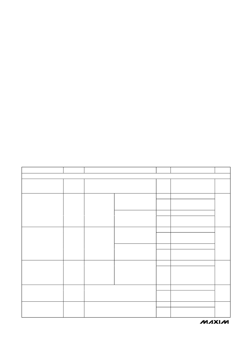
PARAMETER
ANALOG SWITCH
SYMBOL
CONDITIONS
T
A
MIN
TYP
MAX
UNITS
Analog Signal Range
V
COM_
,
V
NO_,
V
NC_
T
MIN
to
T
MAX
0
V+
V
+25°C
0.5
0.85
MAX4755
(NO1, NO2, N_3, N_4),
MAX4754/MAX4756
T
MIN
to
T
MAX
+25°C
1.0
11.5
On-Resistance
R
ON
V+ = 2.7V,
I
COM_
= 10mA,
V
NC
_ =
0V, or
V
NC
_ = V+
(Note 4)
MAX4755 (NC1, NC2)
T
MIN
to
T
MAX
+25°C
8.0
12.5
0.1
0.35
MAX4755
(NO1, NO2, N_3, N_4)
MAX4754/MAX4756
T
MIN
to
T
MAX
+25°C
0.55
0.2
0.4
On-Resistance Match
Between Channels
R
ON
V+ = 2.7V,
I
COM
_ = 10mA,
V
NO
_ = 1.5V, or
V
NC
_ = 1.5V
(Notes 4, 5)
MAX4755 (NC1, NC2)
T
MIN
to
T
MAX
+25°C
0.55
0.2
0.4
On-Resistance Flatness
R
FLAT(ON)
V+ = 3V,
I
COM_
= 10mA,
V
NO_
= 0V, or
V
NC_
= V+
(Note 6)
MAX4755
(NO1, NO2, N_3, N_4,
NO1, NO2),
MAX4754/MAX4756
T
MIN
to
T
MAX
0.55
+25°C
-3
+3
NO_, NC_ Off-Leakage
Current
I
NO_(OFF),
I
NC_(OFF)
V+ = 3.6V;
V
COM_
= 3.3V, 0.3V;
V
NO_
or V
NC_
= 0.3V, 3.3V
T
MIN
to
T
MAX
+25°C
-10
+10
nA
-3
±
0.01
+3
COM_ Off-Leakage
Current
I
COM_(OFF)
V+ = 3.6V (MAX4756);
V
COM_
= 3.3V, 0.3V;
V
NO_
or V
NC_
= 0.3V, 3.3V
T
MIN
to
T
MAX
-10
+10
nA
相關(guān)PDF資料 |
PDF描述 |
|---|---|
| MAX4754EBE-T | 0.5-ohm, QUAD SPDT SWITCHES IN UCSP/QFN |
| MAX4755EBE-T | 0.5-ohm, QUAD SPDT SWITCHES IN UCSP/QFN |
| MAX4755ETE | 0.5-ohm, QUAD SPDT SWITCHES IN UCSP/QFN |
| MAX4756EBE-T | 0.5-ohm, QUAD SPDT SWITCHES IN UCSP/QFN |
| MAX4756ETE | 0.5-ohm, QUAD SPDT SWITCHES IN UCSP/QFN |
相關(guān)代理商/技術(shù)參數(shù) |
參數(shù)描述 |
|---|---|
| MAX4754ETE+ | 功能描述:模擬開關(guān) IC 0.5Ohm Quad SPST Analog Switch RoHS:否 制造商:Texas Instruments 開關(guān)數(shù)量:2 開關(guān)配置:SPDT 開啟電阻(最大值):0.1 Ohms 切換電壓(最大): 開啟時間(最大值): 關(guān)閉時間(最大值): 工作電源電壓:2.7 V to 4.5 V 最大工作溫度:+ 85 C 安裝風(fēng)格:SMD/SMT 封裝 / 箱體:DSBGA-16 |
| MAX4754ETE+T | 功能描述:模擬開關(guān) IC 0.5Ohm Quad SPST Analog Switch RoHS:否 制造商:Texas Instruments 開關(guān)數(shù)量:2 開關(guān)配置:SPDT 開啟電阻(最大值):0.1 Ohms 切換電壓(最大): 開啟時間(最大值): 關(guān)閉時間(最大值): 工作電源電壓:2.7 V to 4.5 V 最大工作溫度:+ 85 C 安裝風(fēng)格:SMD/SMT 封裝 / 箱體:DSBGA-16 |
| MAX4754ETE+WG104 | 制造商:Maxim Integrated Products 功能描述: |
| MAX4754ETE-T | 功能描述:模擬開關(guān) IC RoHS:否 制造商:Texas Instruments 開關(guān)數(shù)量:2 開關(guān)配置:SPDT 開啟電阻(最大值):0.1 Ohms 切換電壓(最大): 開啟時間(最大值): 關(guān)閉時間(最大值): 工作電源電壓:2.7 V to 4.5 V 最大工作溫度:+ 85 C 安裝風(fēng)格:SMD/SMT 封裝 / 箱體:DSBGA-16 |
| MAX4755EBE | 制造商:Rochester Electronics LLC 功能描述: 制造商:Maxim Integrated Products 功能描述: |
發(fā)布緊急采購,3分鐘左右您將得到回復(fù)。