- 您現(xiàn)在的位置:買賣IC網(wǎng) > PDF目錄385530 > MAX4649EKA-T (MAXIM INTEGRATED PRODUCTS INC) 45з, SPDT Analog Switch in SOT23-8 PDF資料下載
參數(shù)資料
| 型號(hào): | MAX4649EKA-T |
| 廠商: | MAXIM INTEGRATED PRODUCTS INC |
| 元件分類: | 運(yùn)動(dòng)控制電子 |
| 英文描述: | 45з, SPDT Analog Switch in SOT23-8 |
| 中文描述: | 1-CHANNEL, SGL POLE DOUBLE THROW SWITCH, PDSO8 |
| 封裝: | SOT-23, 8 PIN |
| 文件頁(yè)數(shù): | 2/10頁(yè) |
| 文件大小: | 216K |
| 代理商: | MAX4649EKA-T |
M
45
, SPDT Analog Switch in SOT23-8
2
_______________________________________________________________________________________
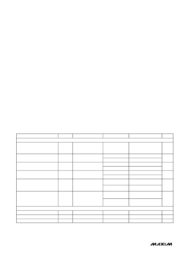
ABSOLUTE MAXIMUM RATINGS
(Voltages referenced to GND.)
ELECTRICAL CHARACTERISTICS—Dual ±15V Supplies
(V+ = +15V, V- = -15V, V
IH
= 2.4V, V
IL
= 0.8V, T
A
= T
MIN
to T
MAX
, unless otherwise noted. Typical values are at T
A
= +25
°
C.) (Notes
2, 3)
Stresses beyond those listed under “Absolute Maximum Ratings” may cause permanent damage to the device. These are stress ratings only, and functional
operation of the device at these or any other conditions beyond those indicated in the operational sections of the specifications is not implied. Exposure to
absolute maximum rating conditions for extended periods may affect device reliability.
V+........................................................................-0.3V to +44.0V
V-.........................................................................-44.0V to +0.3V
V+ to V-................................................................-0.3V to +44.0V
All Other Pins (Note 1)..........................(V- - 0.3V) to (V+ + 0.3V)
Continuous Current into any Terminal..............................±10mA
Continuous Current (COM, NO, NC)................................±30mA
Peak Current (COM, NO, NC)
(pulsed at 1ms, 10% duty cycle)..................................±60mA
Note 1:
Signals on NO, NC, COM, or IN exceeding V+ or V- are clamped by internal diodes. Limit forward-diode current to maxi-
mum current rating.
Continuous Power Dissipation (T
A
= +70
°
C)
8-Pin SOT23 (derate 8.9mW/
°
C above +70
°
C)...........714mW
Operating Temperature Range
MAX4649EKA ............................................-40
°
C to +85
°
C
Storage Temperature Range.............................-65
°
C to +150
°
C
Junction Temperature......................................................+150
°
C
Lead Temperature (soldering, 10s).................................+300
°
C
PARAMETER
SYMBOL
CONDITIONS
T
A
MIN
TYP
MAX
UNITS
ANALOG SWITCH
Analog Signal Range
V
NO
,
V
NC
,
V
COM
V-
V+
V
+25
°
C
33
45
60
5
6
7
10
On-Resistance
R
ON
I
COM
= 1mA; V
NO
or
V
NC
=
±
10V
T
MIN
to T
MAX
+25
°
C
T
MIN
to T
MAX
+25
°
C
T
MIN
to T
MAX
0.6
On-Resistance Matching Between
Channels
R
ON
I
COM
= 1mA; V
NO
or
V
NC
=
±
10V
1.5
On-Resistance Flatness
(Note 4)
R
FLAT
(ON)
I
COM
= 1mA; V
NO
or
V
NC
= +5V, 0, -5V
+25
°
C
-2
0.01
2
NO or NC Off-Leakage
Current
I
NO(OFF)
or
I
NC(OFF)
V
COM
= -14V, +14V;
V
NO
or V
NC
= +14V,
-14V
T
MIN
to T
MAX
-10
10
nA
+25
°
C
-4
4
COM On-Leakage
Current
I
COM(ON)
V
COM
= +14V, -14V;
V
NO
or V
NC
= +14V,
-14V or floating
T
MIN
to T
MAX
-20
20
nA
DIGITAL I/O
Input Logic High Voltage
Input Logic Low Voltage
Input Leakage
V
IH
V
IL
I
IN
2.4
V
V
μ
A
0.8
1
V
IN
= 0 or +5V
-1
相關(guān)PDF資料 |
PDF描述 |
|---|---|
| MAX4655ESA | High-Current, 10ohm, SPST, CMOS Analog Switches |
| MAX4655ETA | High-Current, 10ohm, SPST, CMOS Analog Switches |
| MAX4655EUA | High-Current, 10ohm, SPST, CMOS Analog Switches |
| MAX4656ESA | High-Current, 10ohm, SPST, CMOS Analog Switches |
| MAX4656ETA | High-Current, 10ohm, SPST, CMOS Analog Switches |
相關(guān)代理商/技術(shù)參數(shù) |
參數(shù)描述 |
|---|---|
| MAX464C/D DIE | 制造商:Maxim Integrated Products 功能描述: |
| MAX464CNI | 制造商:Maxim Integrated Products 功能描述: |
| MAX464ENI | 制造商:Maxim Integrated Products 功能描述: |
| MAX464EWI | 功能描述:視頻開關(guān) IC RoHS:否 制造商:Texas Instruments 開關(guān)數(shù)量:4 開啟電阻(最大值):12 Ohms 傳播延遲時(shí)間: 開啟時(shí)間(最大值): 關(guān)閉時(shí)間(最大值): 最大工作溫度:+ 85 C 最小工作溫度:- 40 C 封裝 / 箱體:WQFN-42 封裝:Reel |
| MAX464EWI-T | 功能描述:視頻開關(guān) IC RoHS:否 制造商:Texas Instruments 開關(guān)數(shù)量:4 開啟電阻(最大值):12 Ohms 傳播延遲時(shí)間: 開啟時(shí)間(最大值): 關(guān)閉時(shí)間(最大值): 最大工作溫度:+ 85 C 最小工作溫度:- 40 C 封裝 / 箱體:WQFN-42 封裝:Reel |
發(fā)布緊急采購(gòu),3分鐘左右您將得到回復(fù)。