- 您現(xiàn)在的位置:買(mǎi)賣(mài)IC網(wǎng) > PDF目錄384672 > MAX4389EXT-T (MAXIM INTEGRATED PRODUCTS INC) Ultra-Small, Low-Cost, 85MHz Op Amps with Rail-to-Rail Outputs and Disable PDF資料下載
參數(shù)資料
| 型號(hào): | MAX4389EXT-T |
| 廠商: | MAXIM INTEGRATED PRODUCTS INC |
| 元件分類(lèi): | 音頻/視頻放大 |
| 英文描述: | Ultra-Small, Low-Cost, 85MHz Op Amps with Rail-to-Rail Outputs and Disable |
| 中文描述: | 1 CHANNEL, VIDEO AMPLIFIER, PDSO6 |
| 封裝: | SC-70, 6 PIN |
| 文件頁(yè)數(shù): | 2/19頁(yè) |
| 文件大小: | 734K |
| 代理商: | MAX4389EXT-T |
第1頁(yè)當(dāng)前第2頁(yè)第3頁(yè)第4頁(yè)第5頁(yè)第6頁(yè)第7頁(yè)第8頁(yè)第9頁(yè)第10頁(yè)第11頁(yè)第12頁(yè)第13頁(yè)第14頁(yè)第15頁(yè)第16頁(yè)第17頁(yè)第18頁(yè)第19頁(yè)
M
Ultra-Small, Low-Cost, 85MHz Op Amps with
Rail-to-Rail Outputs and Disable
2
_______________________________________________________________________________________
ABSOLUTE MAXIMUM RATINGS
Supply Voltage (V
CC
to V
EE
)..................................-0.3V to +12V
IN_+, IN_-, OUT_,
DISABLE
.............(V
EE
- 0.3V) to (V
CC
+ 0.3V)
Differential Input Voltage ....................................................±2.5V
Current into Input Pins......................................................±20mA
Output Short-Circuit Duration to
V
CC
or V
EE
(Note 1)................................................Continuous
Continuous Power Dissipation (T
A
= +70
°
C)
5-Pin SOT23 (derate 7.1mW/
°
C above +70
°
C)............571mW
6-Pin SOT23 (derate 8.7mW/
°
C above +70
°
C)............696mW
6-Pin SC70 (derate 3.1mW/
°
C above +70
°
C)..............245mW
Stresses beyond those listed under “Absolute Maximum Ratings” may cause permanent damage to the device. These are stress ratings only, and functional
operation of the device at these or any other conditions beyond those indicated in the operational sections of the specifications is not implied. Exposure to
absolute maximum rating conditions for extended periods may affect device reliability.
8-Pin SO (derate 5.88mW/
°
C above +70
°
C)................471mW
8-Pin μMAX (derate 4.5mW/
°
C above +70
°
C).............362mW
10-Pin μMAX (derate 5.6mW/
°
C above +70
°
C)...........444mW
14-Pin SO (derate 8.33mW/
°
C above +70
°
C)..............667mW
14-Pin TSSOP (derate 10mW/
°
C above +70
°
C) ..........727mW
20-Pin TSSOP (derate 10.9mW/
°
C above +70
°
C) .......879mW
Operating Temperature Range ...........................-40
°
C to +85
°
C
Junction Temperature......................................................+150
°
C
Storage Temperature Range.............................-65
°
C to +150
°
C
Lead Temperature (soldering, 10s).................................+300
°
C
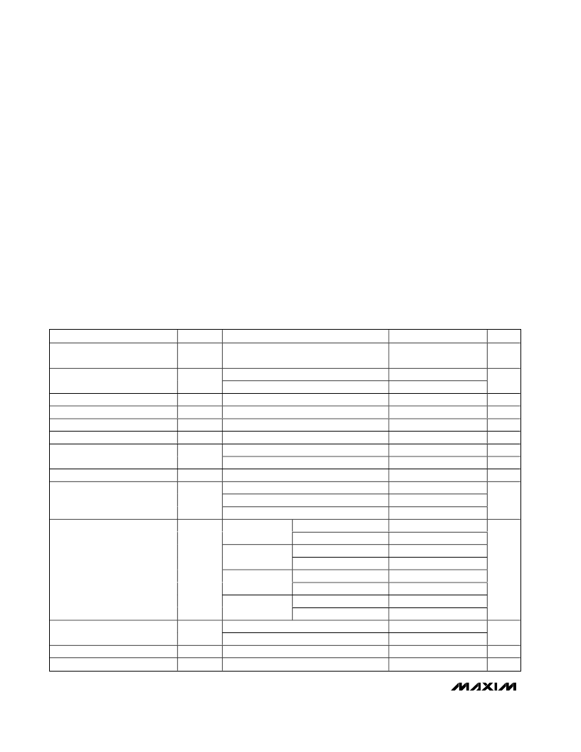
DC ELECTRICAL CHARACTERISTICS
—
Single Supply
(V
CC
= 5V, V
EE
= 0V, V
CM
= V
CC
/2, V
OUT
= V
CC
/2, R
L
=
∞
to V
CC
/2,
DISABLE_
= V
CC
(MAX4389/MAX4393/MAX4394/MAX4396),
T
A
= T
MIN
to T
MAX
, unless otherwise noted. Typical values are at T
A
= +25
°
C.) (Note 2)
PARAMETER
SYMBOL
CONDITIONS
MIN
TYP
MAX
UNITS
Input Common-Mode Voltage
Range
V
CM
Guaranteed by CMRR test
V
EE
-
0.2
V
CC
-
2.25
V
T
A
= +25
°
C
TA = -40
°
C to +85
°
C
MAX4392
–
MAX4396
5
18
26
Input Offset Voltage
V
OS
mV
Input Offset Voltage Matching
Input Offset Voltage Tempco
Input Bias Current
Input Offset Current
1
15
2.5
0.2
70
3
95
70
60
58
0.065
0.05
0.3
0.25
0.5
0.45
1
0.025
55
50
±
100
8
mV
μV/
°
C
μA
μA
k
M
dB
TC
VOS
I
B
IOS
15
5
Differential mode (-1V
≤
V
IN
≤
+1V)
Common mode (-0.2V
≤
V
CM
≤
+2.75V)
(V
EE
- 0.2V)
≤
V
CM
≤
(V
CC
- 2.25V)
0.25V
≤
V
OUT
≤
4.75V, R
L
= 2k
0.8V
≤
V
OUT
≤
4.5V, R
L
= 150
1V
≤
V
OUT
≤
4V, R
L
= 50
Input Resistance
R
IN
Common-Mode Rejection Ratio
CMRR
70
50
50
Open-Loop Gain
A
VOL
dB
V
CC
- V
OH
V
OL
- V
EE
V
CC
- V
OH
V
OL
- V
EE
V
CC
- V
OH
V
OL
- V
EE
V
CC
- V
OH
V
OL
- V
EE
0.25
0.15
0.5
0.5
0.8
0.8
1.7
0.1
R
L
= 2k
R
L
= 150
R
L
= 75
Output Voltage Swing
V
OUT
R
L
= 75
to
ground
V
Sinking from R
L
= 75
to V
CC
Sourcing into R
L
= 75
to V
EE
Sinking or sourcing
40
40
Output Current
I
OUT
mA
Output Short-Circuit Current
Open-Loop Output Resistance
I
SC
R
OUT
mA
Note 1:
Continuous power dissipation must also be observed.
相關(guān)PDF資料 |
PDF描述 |
|---|---|
| MAX4397DCTM | Audio/Video Switch For Dual SCART Connectors |
| MAX4397 | Audio/Video Switch For Dual SCART Connectors |
| MAX4397D | Audio/Video Switch For Dual SCART Connectors |
| MAX4397S | Audio/Video Switch For Dual SCART Connectors |
| MAX4397SCTM | Audio/Video Switch For Dual SCART Connectors |
相關(guān)代理商/技術(shù)參數(shù) |
參數(shù)描述 |
|---|---|
| MAX438C/D DIE | 制造商:Maxim Integrated Products 功能描述: |
| MAX4390EUK | 制造商:Maxim Integrated Products 功能描述:ULTRA-SMALL LOW-COST 145MHZ OP AM - Cut Tape Product 制造商:Rochester Electronics LLC 功能描述: |
| MAX4390EUK+ | 制造商:Maxim Integrated Products 功能描述:OP AMP SGL VOLT FDBK R-R O/P 5.5V/11V 5PIN SOT-23 - Rail/Tube |
| MAX4390EUK+T | 功能描述:高速運(yùn)算放大器 85MHz w/Rail-Rail Output RoHS:否 制造商:Texas Instruments 通道數(shù)量:1 電壓增益 dB:116 dB 輸入補(bǔ)償電壓:0.5 mV 轉(zhuǎn)換速度:55 V/us 工作電源電壓:36 V 電源電流:7.5 mA 最大工作溫度:+ 85 C 安裝風(fēng)格:SMD/SMT 封裝 / 箱體:SOIC-8 封裝:Tube |
| MAX4390EUK+TG126 | 功能描述:運(yùn)算放大器 - 運(yùn)放 Ultra-Small Low-Cost 85MHz Op Amps with Rail-to-Rail Outputs and Disable RoHS:否 制造商:STMicroelectronics 通道數(shù)量:4 共模抑制比(最小值):63 dB 輸入補(bǔ)償電壓:1 mV 輸入偏流(最大值):10 pA 工作電源電壓:2.7 V to 5.5 V 安裝風(fēng)格:SMD/SMT 封裝 / 箱體:QFN-16 轉(zhuǎn)換速度:0.89 V/us 關(guān)閉:No 輸出電流:55 mA 最大工作溫度:+ 125 C 封裝:Reel |
發(fā)布緊急采購(gòu),3分鐘左右您將得到回復(fù)。