- 您現(xiàn)在的位置:買賣IC網(wǎng) > PDF目錄383370 > MAX362MJE (MAXIM INTEGRATED PRODUCTS INC) Precision, Quad, SPST Analog Switches PDF資料下載
參數(shù)資料
| 型號: | MAX362MJE |
| 廠商: | MAXIM INTEGRATED PRODUCTS INC |
| 元件分類: | 運動控制電子 |
| 英文描述: | Precision, Quad, SPST Analog Switches |
| 中文描述: | QUAD 1-CHANNEL, SGL POLE SGL THROW SWITCH, CDIP16 |
| 封裝: | CERDIP-16 |
| 文件頁數(shù): | 6/8頁 |
| 文件大小: | 99K |
| 代理商: | MAX362MJE |
M
Prec ision, Quad, S PS T Analog S witc hes
6
_______________________________________________________________________________________
____________________________Typic al Operating Charac teristic s (c ontinued)
(T
A
= +25°C, unless otherwise noted.)
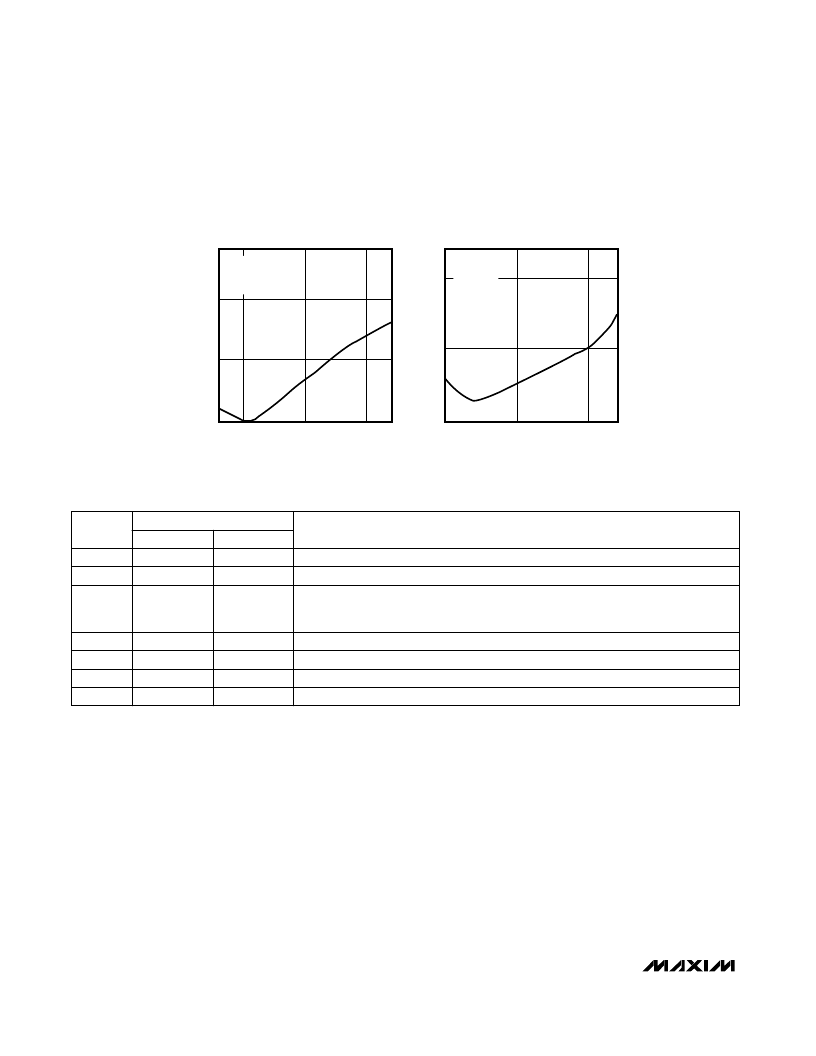
CHARGE INJECTION vs.
VCOM VOLTAGE
Q
-20
0
20
40
-14
-10
0
10
14
V
COM
(V)
V+ = 15V
V- = -15V
CL = 1nF
CHARGE INJECTION vs.
VCOM VOLTAGE
Q
-10
0
10
0
5
10
12
V
COM
(V)
V+ = 12V
V- = 0V
CL = 1nF
___________Applic ations Information
Operation with S upply V oltages
Other T han ±15V
O
Using supply voltages other than ±15V is reduces the
analog signal range. The MAX361/MAX362 switches
operate with bipolar supplies of ±4.5V to ±20V. Typical
operating characteristic graphs show typical on resis-
tance for ±15V, ±10V, and ±5V supplies. Switching
times increase by a factor of two or more for ±5V oper-
ation. The MAX361/MAX362 can also operate from
+10V to +30V unipolar supplies. Both parts can also
be powered from unbalanced supplies such as +24V
and -5V. Connect V- to 0V when operating with a sin-
gle supply.
Proper power-supply sequencing is recommended for
all CMOS devices. Do not exceed the absolute maxi-
mum ratings, because stresses beyond the listed rat-
ings may cause permanent damage to the devices.
Always sequence V+ on first, followed by V-, and logic
inputs. If power-supply sequencing is not possible,
add two small signal diodes in series with the supply
pins for overvoltage protection (Figure 6). Adding the
diodes reduces the analog signal range to 1V below
V+ and 1V below V-, but low switch resistance and low
leakage characteristics are unaffected. Device opera-
tion is unchanged, and the difference from V+ to V-
should not exceed +44V.
PIN
NAME
MAX361
IN1-IN4
COM1-COM4
MAX362
IN1-IN4
COM1-COM4
FUNCTION
1, 16, 9, 8
2, 15, 10, 7
Logic-level input
Analog switch common terminal
NC (normally closed, MAX361)
NO (normally open, MAX362)
Analog switch terminal
Negative supply voltage input
Ground
Not internally connected
Positive supply voltage input—connected to substrate.
3, 14, 11, 6
NC1-NC4
NO1-NO4
4
5
V-
V-
GND
N.C.
V+
GND
N.C.
V+
12
13
______________________________________________________________Pin Desc ription
相關(guān)PDF資料 |
PDF描述 |
|---|---|
| MAX364-MAX365 | Precision, Quad, SPST Analog Switches |
| MAX365CPE | Precision, Quad, SPST Analog Switches |
| MAX365CSE | Precision, Quad, SPST Analog Switches |
| MAX365EPE | Precision, Quad, SPST Analog Switches |
| MAX365ESE | Precision, Quad, SPST Analog Switches |
相關(guān)代理商/技術(shù)參數(shù) |
參數(shù)描述 |
|---|---|
| MAX362MJE/883B | 制造商:Maxim Integrated Products 功能描述:- Bulk |
| MAX3632ETG | 制造商:Maxim Integrated Products 功能描述:622MBPS/1244MBPS BURST-MODE LIMITING AMPLIFIE - Rail/Tube |
| MAX3632ETG+ | 制造商:Maxim Integrated Products 功能描述:622MBPS/1244MBPS BURST-MODE LIMITING AMPLIFIER FOR GPON OLT - Rail/Tube |
| MAX3632ETG+T | 制造商:Maxim Integrated Products 功能描述:622MBPS/1244MBPS BURST-MODE LIMITING AMPLIFIER FOR GPON OLT - Tape and Reel |
| MAX3632ETG-T | 制造商:Maxim Integrated Products 功能描述:622MBPS/1244MBPS BURST-MODE LIMITING AMPLIFIE - Tape and Reel |
發(fā)布緊急采購,3分鐘左右您將得到回復(fù)。