- 您現(xiàn)在的位置:買賣IC網(wǎng) > PDF目錄384656 > MAX2101CMQ (MAXIM INTEGRATED PRODUCTS INC) 16-Bit Buffers/Drivers With 3-State Outputs 48-TSSOP -40 to 85 PDF資料下載
參數(shù)資料
| 型號: | MAX2101CMQ |
| 廠商: | MAXIM INTEGRATED PRODUCTS INC |
| 元件分類: | 消費家電 |
| 英文描述: | 16-Bit Buffers/Drivers With 3-State Outputs 48-TSSOP -40 to 85 |
| 中文描述: | SPECIALTY CONSUMER CIRCUIT, PQFP100 |
| 封裝: | METRIC, QFP-100 |
| 文件頁數(shù): | 19/24頁 |
| 文件大小: | 217K |
| 代理商: | MAX2101CMQ |
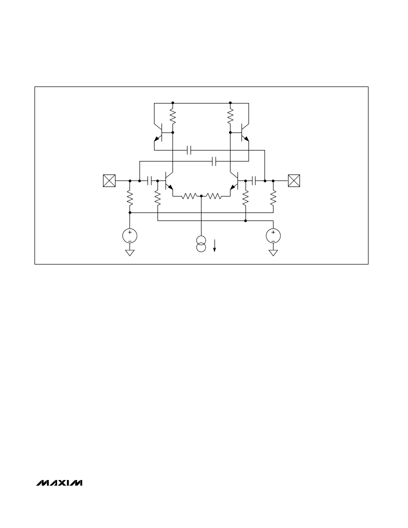
performance in the specification, the resonant network
should exhibit a loaded Q greater than 20.
The resonating inductor L
RES
should exhibit as high a
Q factor as is reasonably possible. The inductor’s self-
resonant frequency (SRF) should be well in excess of
the intended frequencies of operation. An air-wound
design is a simple example of an inductor that would fit
these criteria.
A dual varactor topology is recommended for C
VAR
to
compensate for the large-signal amplitude incident
across the resonator ports. The dual varactor in the
arrangement shown in Figure 5 (to first order) allows
cancellation of capacitance modulation due to the large
signals, as the two diodes are driven in a complemen-
tary fashion by the LO signal. The dual varactor design
also allows use of devices with larger C
O
values, sim-
plifying device selection. The varactor should be driven
with a large reverse bias to increase the MAX2101’s
effective Q.
The resonant frequency is primarily determined by
C
SH
, which shunts the varactor diodes. C
SH
is trimmed
(selected) to determine the approximate tuning range
of the phase-locked loop. For applications relevant to
the MAX2101, this frequency range can cover the UHF
spectrum from 400MHz to 700MHz. The varactor within
the loop will then determine the actual LO frequency
within a much narrower tuning range. Depending on
the expected tuning range variation, C
SH
could be
made of a combination of fixed capacitance and
trimmed capacitance. This shunt capacitance will
increase the loaded Q of the resonator and lower the V
to F gain constant, improving the oscillator’s phase-
noise performance.
The coupling capacitors C
C
couple the variable capac-
itor network to the tank ports and resonating inductor.
These elements should be selected to present low
impedance (less than 1
) at the lowest expected oper-
ating frequency. These capacitors should also exhibit
low effective series resistance (ESR) to maintain a high
resonator-loaded Q. R
CHOKE
provides a DC bias for
the varactors, while ensuring a high impedance at the
intended operating frequency. The magnitude of the
choke network’s series impedance should be approxi-
mately 10 times the resonant inductor’s impedance at
the operating frequency. Resistors R
BUF
provide drive
for the varactor while ensuring adequate isolation
between the two differential resonator ports. C
FLTR
, in
combination with R
BUF,
provides additional filtering of
the drive signal from the loop.
M
6-Bit Quadrature Digitizer
______________________________________________________________________________________
19
R
B2
R
I
I
EE
R
B1
TNKB
(PIN 14)
V
B2
R
B1
TNKA
(PIN 17)
V
B1
R
B2
R
I
C
C
C
C
R
E
R
E
C
F
C
F
V
CC
Figure 15. Simplified Input Network for VCO Resonator Ports
相關(guān)PDF資料 |
PDF描述 |
|---|---|
| MAX2102 | 16-Bit Buffers/Drivers With 3-State Outputs 48-TVSOP -40 to 85 |
| MAX2102-MAX2105 | Direct-Conversion Tuner ICs for Digital DBS Applications |
| MAX2105 | 16-Bit Buffers/Drivers With 3-State Outputs 48-TSSOP -40 to 85 |
| MAX2105CWI | Direct-Conversion Tuner ICs for Digital DBS Applications |
| MAX2104 | 16-Bit Buffers/Drivers With 3-State Outputs 48-TSSOP -40 to 85 |
相關(guān)代理商/技術(shù)參數(shù) |
參數(shù)描述 |
|---|---|
| MAX2102 | 制造商:MAXIM 制造商全稱:Maxim Integrated Products 功能描述:Evaluation Kit |
| MAX2102/MAX2105 | 制造商:MAXIM 制造商全稱:Maxim Integrated Products 功能描述:Direct-Conversion Tuner ICs for Digital DBS Applications |
| MAX2102_1 | 制造商:MAXIM 制造商全稱:Maxim Integrated Products 功能描述:Evaluation Kit |
| MAX2102CWI | 制造商:Rochester Electronics LLC 功能描述: 制造商:Maxim Integrated Products 功能描述: |
| MAX2102CWI.B50030 | 制造商:Maxim Integrated Products 功能描述: |
發(fā)布緊急采購,3分鐘左右您將得到回復(fù)。