- 您現(xiàn)在的位置:買賣IC網(wǎng) > PDF目錄383338 > MAX1855EEG (MAXIM INTEGRATED PRODUCTS INC) Replaced by TMS320C6202B : Fixed-Point Digital Signal Processor 352-FCBGA PDF資料下載
參數(shù)資料
| 型號: | MAX1855EEG |
| 廠商: | MAXIM INTEGRATED PRODUCTS INC |
| 元件分類: | 穩(wěn)壓器 |
| 英文描述: | Replaced by TMS320C6202B : Fixed-Point Digital Signal Processor 352-FCBGA |
| 中文描述: | SWITCHING CONTROLLER, 550 kHz SWITCHING FREQ-MAX, PDSO24 |
| 封裝: | 0.150 INCH, 0.025 INCH PITCH, QSOP-24 |
| 文件頁數(shù): | 19/33頁 |
| 文件大小: | 840K |
| 代理商: | MAX1855EEG |
第1頁第2頁第3頁第4頁第5頁第6頁第7頁第8頁第9頁第10頁第11頁第12頁第13頁第14頁第15頁第16頁第17頁第18頁當(dāng)前第19頁第20頁第21頁第22頁第23頁第24頁第25頁第26頁第27頁第28頁第29頁第30頁第31頁第32頁第33頁
M
High-Speed, Adjustable, Synchronous Step-Down
Controllers with Integrated Voltage Positioning
______________________________________________________________________________________
19
V
CC
. The logic threshold for switchover to the 120mV
default value is approximately V
CC
- 1V.
Carefully observe the PC board layout guidelines to
ensure that noise and DC errors don
’
t corrupt the cur-
rent-sense signals seen by CS and PGND. The IC must
be mounted close to the current-sense resistor with
short, direct traces making a Kelvin sense connection.
MOSFET Gate Drivers (DH and DL)
The DH and DL drivers are optimized for driving mod-
erate-sized, high-side and larger, low-side power
MOSFETs. This is consistent with the low duty factor
seen in the notebook CPU environment, where a large
V
IN
- V
OUT
differential exists. An adaptive dead-time
circuit monitors the DL output and prevents the high-
side FET from turning on until DL is fully off. There must
be a low-resistance, low-inductance path from the DL
driver to the MOSFET gate in order for the adaptive
dead-time circuit to work properly. Otherwise, the
sense circuitry in the MAX1716/MAX1854/MAX1855 will
interpret the MOSFET gate as
“
off
”
while there is actual-
ly still charge left on the gate. Use very short, wide
traces measuring 10 to 20 squares (50 to 100 mils wide
if the MOSFET is 1 inch from the device). The dead
time at the other edge (DH turning off) is determined by
a fixed 35ns internal delay.
The internal pulldown transistor that drives DL low is
robust, with a 0.5
(typ) on-resistance. This helps pre-
vent DL from being pulled up during the fast rise time
of the LX node, due to capacitive coupling from the
drain to the gate of the low-side synchronous-rectifier
MOSFET. However, for high-current applications, some
combinations of high- and low-side FETs may cause
excessive gate-drain coupling, leading to poor efficien-
cy, EMI, and shoot-through currents. This is often reme-
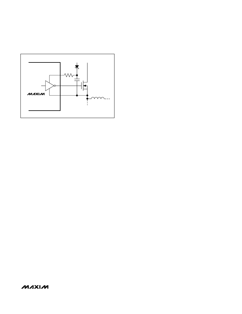
died by adding a resistor in series with BST, which
increases the turn-on time of the high-side FET without
degrading the turn-off time (Figure 5).
DAC Converter (D0–D4)
The digital-to-analog converter (DAC) programs the
output voltage. It receives a preset digital code from
the VID inputs (D0
–
D4), which contain weak internal
pullups to eliminate external resistors. They can also be
driven by digital logic, general-purpose I/O, or an exter-
nal multiplexer. The available DAC codes and resulting
output voltages (Table 5) are compatible with Intel
’
s
mobile Pentium III
specifications.
D0-D4 can be changed while the regulator is active, ini-
tiating a transition to a new output voltage level.
Change D0
–
D4 synchronously to avoid errors during a
V
OUT
transition. If the skew between bits exceeds 1μs,
incorrect DAC outputs may cause a partial transition to
the wrong voltage level, followed by the intended tran-
sition to the correct voltage level, lengthening the over-
all transition time.
When changing the MAX1855 DAC code while pow-
ered up, the undervoltage protection feature can be
activated if the code change increases the output volt-
age by more than 120%. For example, a transition from
any DAC code below 0.8V to 1.75V will activate the
undervoltage protection. In the preceding example,
transitioning from 0.8V to 1.35V and then from 1.35V to
1.75V avoids activating the undervoltage protection
feature.
Shutdown (
SHDN
)
Drive
SHDN
low to force the MAX1716/MAX1854/
MAX1855 into a low-current shutdown state. Shutdown
turns on the low-side MOSFET by forcing the DL gate
driver high, which discharges the output capacitor and
forces the output to ground. Drive or connect
SHDN
to
V
CC
for normal operation. A rising edge on
SHDN
clears the fault latch.
Power-on Reset
Power-on reset (POR) occurs when V
CC
rises above
approximately 2V. This resets the fault latch and soft-
start counter, preparing the regulator for operation.
BST
+5V
V
BATT
5
TYP
DH
LX
MAX1716
MAX1854
MAX1855
Figure 5. Reducing the Switching-Node Rise Time
Pentium III is a trademark of Intel Corp.
相關(guān)PDF資料 |
PDF描述 |
|---|---|
| MAX1854 | High-Speed, Adjustable, Synchronous Step-Down Controllers with Integrated Voltage Positioning |
| MAX1857EUA47 | 500mA, Low-Dropout, Ripple-Rejecting LDO in MAX |
| MAX1857 | Replaced by TMS320C6202B : Fixed-Point Digital Signal Processor 352-FCBGA |
| MAX1858 | Dual 180∑ Out-of-Phase Buck Controllers with Sequencing/Prebias Startup and POR |
| MAX1858EEG | Dual 180∑ Out-of-Phase PWM Step-Down Controller with Power Sequencing and POR |
相關(guān)代理商/技術(shù)參數(shù) |
參數(shù)描述 |
|---|---|
| MAX1855EEG+ | 制造商:Rochester Electronics LLC 功能描述: 制造商:Maxim Integrated Products 功能描述: |
| MAX1855EEG-T | 功能描述:DC/DC 開關(guān)控制器 RoHS:否 制造商:Texas Instruments 輸入電壓:6 V to 100 V 開關(guān)頻率: 輸出電壓:1.215 V to 80 V 輸出電流:3.5 A 輸出端數(shù)量:1 最大工作溫度:+ 125 C 安裝風(fēng)格: 封裝 / 箱體:CPAK |
| MAX1855EVKIT | 功能描述:DC/DC 開關(guān)控制器 Evaluation Kit for the MAX1716 MAX1854 MAX1855 RoHS:否 制造商:Texas Instruments 輸入電壓:6 V to 100 V 開關(guān)頻率: 輸出電壓:1.215 V to 80 V 輸出電流:3.5 A 輸出端數(shù)量:1 最大工作溫度:+ 125 C 安裝風(fēng)格: 封裝 / 箱體:CPAK |
| MAX1856EUB | 功能描述:電信線路管理 IC RoHS:否 制造商:STMicroelectronics 產(chǎn)品:PHY 接口類型:UART 電源電壓-最大:18 V 電源電壓-最小:8 V 電源電流:30 mA 最大工作溫度:+ 85 C 最小工作溫度:- 40 C 安裝風(fēng)格:SMD/SMT 封裝 / 箱體:VFQFPN-48 封裝:Tray |
| MAX1856EUB+ | 功能描述:電信線路管理 IC Synchronizable PWM SLIC Power Supply RoHS:否 制造商:STMicroelectronics 產(chǎn)品:PHY 接口類型:UART 電源電壓-最大:18 V 電源電壓-最小:8 V 電源電流:30 mA 最大工作溫度:+ 85 C 最小工作溫度:- 40 C 安裝風(fēng)格:SMD/SMT 封裝 / 箱體:VFQFPN-48 封裝:Tray |
發(fā)布緊急采購,3分鐘左右您將得到回復(fù)。