- 您現(xiàn)在的位置:買賣IC網(wǎng) > PDF目錄384654 > MAX1817EUB (MAXIM INTEGRATED PRODUCTS INC) Replaced by TMS320VC5506 : Digital Signal Processors 132-BQFP -40 to 85 PDF資料下載
參數(shù)資料
| 型號: | MAX1817EUB |
| 廠商: | MAXIM INTEGRATED PRODUCTS INC |
| 元件分類: | 穩(wěn)壓器 |
| 英文描述: | Replaced by TMS320VC5506 : Digital Signal Processors 132-BQFP -40 to 85 |
| 中文描述: | 1.05 A SWITCHING REGULATOR, 500 kHz SWITCHING FREQ-MAX, PDSO10 |
| 封裝: | UMAX-10 |
| 文件頁數(shù): | 10/12頁 |
| 文件大小: | 403K |
| 代理商: | MAX1817EUB |
M
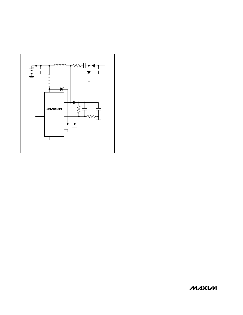
Using a Charge Pump to Make Negative
LCD Output Voltage
The MAX1817 can generate a negative LCD output by
adding a diode-capacitor charge-pump circuit (D3, D4,
and C6) to the LXLCD pin as shown in Figure 4. FBLCD
is driven through a resistive voltage-divider from the
positive output, which is not loaded, allowing a very
small capacitor value at C2. For best stability and low-
est ripple, the time constant of the R1 + R2 series com-
bination and C2 should be near that of C5 and the
effective load resistance. Output load regulation of the
negative output degrades compared to the standard
positive output circuit and may rise at very light loads. If
this is not acceptable, reduce the resistance of R1 and
R2, while maintaining their ratio, to effectively preload
the output with a few hundred μA. This is why the R1
and R2 values shown in Figure 4 are lower than typical
values for a positive-output design. When loaded, the
magnitude of the negative output voltage is slightly
lower (closer to ground by approximately a diode for-
ward voltage) than the voltage on C2.
Applications Information
Inductor Selection
The MAX1817
’
s high switching frequency allows the
use of small surface-mount inductors. The 10μH values
shown in Figure 3 are recommended for most applica-
tions, although values between 4.7μH and 47μH are
suitable. Smaller inductance values typically offer a
smaller physical size for a given series resistance,
allowing the smallest overall circuit dimensions. Larger
inductance values exhibit higher output current capa-
bility, but larger physical dimensions.
Circuits using larger inductance values may start up at
lower input voltages and exhibit less ripple, but they
may provide reduced output power. This occurs when
the inductance is sufficiently large to prevent the maxi-
mum current limit from being reached before the maxi-
mum on-time expires. The inductor
’
s saturation current
rating should be greater than the peak switching cur-
rent. However, it is generally acceptable to bias most
inductors into saturation by as much as 20%, although
this may slightly reduce efficiency.
For best efficiency, select inductors with resistance no
greater than the internal N-channel FET resistance in
each step-up converter.
For maximum output current, choose L such that:
L < [(V
IN
t
ON
) / I
PEAK
]
where t
ON
is the maximum switch on-time (5μs for main
step-up converter) or 9μs for LCD step-up converter)
and I
PEAK
is the switch peak current limit (0.75A for the
main step-up converter, or 0.5A for the LCD step-up
converter). With this inductor value, the maximum output
current the main converter is able to deliver is given by:
I
OUT(MAX)
= 0.5
I
PEAK
/ (1 + t
ON
/ t
OFF
)
where t
ON
/ t
OFF
= (V
OUT
+ V
D
- V
IN
) / (V
IN
- V
ON
), V
IN
and V
OUT
are the input and output voltages, V
D
is the
Schottky diode drop (0.3V typ), and V
ON
= I
PEAK
R
ON
, where R
ON
is the switch on-resistance.
For V
IN
= 1.5V and V
OUT
= 3.3V, with a minimum I
PEAK
value of 0.5A, and V
ON(MAX)
given by (0.5)
(0.65) =
0.325V, the available output current that the converter
can provide is at least 90mA.
For larger inductor values, I
PEAK
is determined by:
I
PEAK
= [(V
IN
t
ON
) / L]
External Rectifiers
The high maximum switching frequency of the
MAX1817 requires a high-speed rectifier. Schottky
diodes such as the Motorola MBR0530 or the Nihon
EP05Q03L are recommended. To maintain high effi-
ciency, the average current rating of the Schottky diode
should be greater than the peak switching current. A
junction diode such as the Central Semiconductor
CMPD4448 can be used for the LCD output with little
Compact, High-Efficiency, Dual-Output
Step-Up DC-DC Converter
10
______________________________________________________________________________________
MAX1817
ONLCD
LX
ON
FB
OUT
FBLCD
V
IN
MAIN
-19V
V
LCD
C5
1
μ
F
R2
16.5k
R1
240k
R3
1
D1**
D2
D3*
D4*
C1
10
μ
F
L2
10
μ
H
L1,10
μ
H
C2
0.1
μ
F
C3
22
μ
F
C4
10pF
C6
0.1
μ
F
AGND
GND
LXLCD
*D3, D4 = CENTRAL SEMICONDUCTOR
CMPD7000 DUAL
**D1 = CENTRAL SEMICONDUCTOR
CMSD4448 (1N4148)
Figure 4. Negative Voltage for LCD Bias
相關(guān)PDF資料 |
PDF描述 |
|---|---|
| MAX1822 | High-Side Power Supply |
| MAX1822ESA | High-Side Power Supply |
| MAX1823 | Dual USB Switch with Fault Blanking and Autoreset |
| MAX1823AEUB | Replaced by TMS320BC52 : |
| MAX1823BEUB | Replaced by TMS320BC52 : |
相關(guān)代理商/技術(shù)參數(shù) |
參數(shù)描述 |
|---|---|
| MAX1817EUB+ | 功能描述:直流/直流開關(guān)轉(zhuǎn)換器 Dual-Output Step-Up DC/DC Converter RoHS:否 制造商:STMicroelectronics 最大輸入電壓:4.5 V 開關(guān)頻率:1.5 MHz 輸出電壓:4.6 V 輸出電流:250 mA 輸出端數(shù)量:2 最大工作溫度:+ 85 C 安裝風格:SMD/SMT |
| MAX1817EUB+T | 功能描述:直流/直流開關(guān)轉(zhuǎn)換器 Dual-Output Step-Up DC/DC Converter RoHS:否 制造商:STMicroelectronics 最大輸入電壓:4.5 V 開關(guān)頻率:1.5 MHz 輸出電壓:4.6 V 輸出電流:250 mA 輸出端數(shù)量:2 最大工作溫度:+ 85 C 安裝風格:SMD/SMT |
| MAX1817EUB-T | 功能描述:直流/直流開關(guān)轉(zhuǎn)換器 Dual-Output Step-Up DC/DC Converter RoHS:否 制造商:STMicroelectronics 最大輸入電壓:4.5 V 開關(guān)頻率:1.5 MHz 輸出電壓:4.6 V 輸出電流:250 mA 輸出端數(shù)量:2 最大工作溫度:+ 85 C 安裝風格:SMD/SMT |
| MAX1817EVKIT | 制造商:Maxim Integrated Products 功能描述:COMPACT, HIGH-EFFICIENCY, DUAL-OUTPUT STEP-UP - Bulk |
| MAX1818ESA20 | 制造商:Rochester Electronics LLC 功能描述: 制造商:Maxim Integrated Products 功能描述: |
發(fā)布緊急采購,3分鐘左右您將得到回復(fù)。