- 您現(xiàn)在的位置:買賣IC網(wǎng) > PDF目錄383311 > MAX1160ACWI (MAXIM INTEGRATED PRODUCTS INC) 10-Bit, 20Msps, TTL-Output ADC PDF資料下載
參數(shù)資料
| 型號: | MAX1160ACWI |
| 廠商: | MAXIM INTEGRATED PRODUCTS INC |
| 元件分類: | ADC |
| 英文描述: | 10-Bit, 20Msps, TTL-Output ADC |
| 中文描述: | 1-CH 10-BIT PROPRIETARY METHOD ADC, PARALLEL ACCESS, PDSO28 |
| 封裝: | 0.300 INCH, PLASTIC, MS-013AE, SOIC-28 |
| 文件頁數(shù): | 6/8頁 |
| 文件大小: | 76K |
| 代理商: | MAX1160ACWI |

The MAX1160 has two grounds: AGND and DGND.
These internal grounds are isolated on the device. Use
ground planes for optimum device performance. Use
DGND for the DV
CC
return path (typically 40mA) and
for the return path for all digital output logic interfaces.
Separate AGND and DGND from each other, connect-
ing them together only through a ferrite bead at the
device.
Connect a Schottky or hot carrier diode between AGND
and V
EE
. The use of separate power supplies between
V
CC
and DV
CC
is not recommended due to potential
power-supply-sequencing latchup conditions. For opti-
mum performance, use the recommended circuit
shown in Figure 2.
V oltage Referenc e
The MAX1160 requires the use of two voltage refer-
ences: VFT and VFB. VFT is the force for the top of the
voltage-reference ladder (typically +2.5V); VFB (typical-
ly -2.5V) is the force for the bottom of the voltage-refer-
ence ladder. Both voltages are applied across an 800
internal reference-ladder resistance. The +2.5V voltage
source for reference VFT must be current limited to
20mA (max) if a different driving circuit is used in place
of the recommended reference circuit shown in Figures
2 and 3. In addition, there are three reference-ladder
taps (VST, VRM, and VSB). VST is the sense for the top
of the reference ladder (+2V), VRM is the midpoint of
the ladder (typically 0V), and VSB is the sense for the
bottom of the reference ladder (-2V). The voltages at
VST and VSB are the device’s true full-scale input volt-
ages when VFT and VFB are driven to the recommend-
ed voltages (typically +2.5V and -2.5V, respectively).
These points should be used to monitor the device’s
actual full-scale input range. When not being used, a
decoupling capacitor of 0.01μF (chip capacitor pre-
ferred) connected to AGND from each tap is recom-
mended to minimize high-frequency noise injection.
Figure 2 shows an example of a recommended refer-
ence-driver circuit. IC1 is a MAX6225, a 2.5V reference
with an accuracy of 0.2%. The 10k
potentiometer R1
supports a minimum adjustable range of 0.6%. Use an
OP07 or equivalent device for IC2. R2 and R3 must be
matched to within 0.1% with good TC tracking to main-
tain 0.3LSB matching between VFT and VFB. If 0.1%
matching is not met, then R4 can be used to adjust the
VFB voltage to the desired level. Adjust VFT and VFB
such that VST and VSB are exactly +2V and -2V,
respectively.
The analog input range scales proportionally with respect
to the reference voltage if a different input range is
required. The maximum scaling factor for device opera-
tion is ±20% of the recommended reference voltages of
VFT and VFB. However, because the device is laser
trimmed to optimize performance with ±2.5V references,
its accuracy degrades if operated beyond a ±2% range.
M
10-Bit, 20Msps, T T L-Output ADC
6
_______________________________________________________________________________________
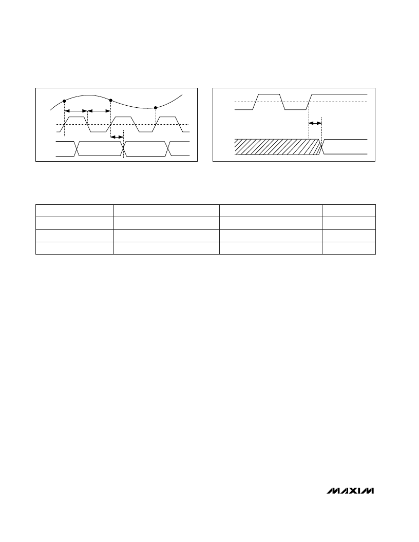
CLK
t
pwH
N - 2
N - 1
N
DATA VALID
N
DATA VALID
N + 1
t
pwL
t
d
N + 1
N + 2
OUTPUT
DATA
Figure 1a. Timing Diagram
CLK
DATA VALID
t
d
OUTPUT
DATA
Figure 1b. Single-Event Clock
Table 1. Timing Parameters
DESCRIPTION
UNITS
t
d
CLK to Data Valid Propagation Delay
ns
t
pwH
CLK High Pulse Width
ns
PARAMETER
20
300
t
pwL
CLK Low Pulse Width
ns
20
MIN
TYP
MAX
14
18
相關PDF資料 |
PDF描述 |
|---|---|
| MAX1160BCPI | 10-Bit, 20Msps, TTL-Output ADC |
| MAX1160BCWI | 10-Bit, 20Msps, TTL-Output ADC |
| MAX1168AEEG | Multichannel, 16-Bit, 200ksps Analog-to-Digital Converters |
| MAX1167 | Multichannel. 16-Bit. 200ksps Analog-to-Digital Converters |
| MAX1168 | Multichannel. 16-Bit. 200ksps Analog-to-Digital Converters |
相關代理商/技術參數(shù) |
參數(shù)描述 |
|---|---|
| MAX1160BCPI | 制造商:MAXIM 制造商全稱:Maxim Integrated Products 功能描述:10-Bit, 20Msps, TTL-Output ADC |
| MAX1160BCWI | 制造商:MAXIM 制造商全稱:Maxim Integrated Products 功能描述:10-Bit, 20Msps, TTL-Output ADC |
| MAX1161 | 制造商:MAXIM 制造商全稱:Maxim Integrated Products 功能描述:10-Bit, 40Msps, TTL-Output ADC |
| MAX11610 | 制造商:MAXIM 制造商全稱:Maxim Integrated Products 功能描述:2.7V to 3.6V and 4.5V to 5.5V, Low-Power, 4-/8-/12-Channel, 2-Wire Serial 10-Bit ADCs |
| MAX11610EEE+ | 功能描述:模數(shù)轉(zhuǎn)換器 - ADC 10-Bit 12Ch 94.4sps 5.5V Precision ADC RoHS:否 制造商:Texas Instruments 通道數(shù)量:2 結(jié)構(gòu):Sigma-Delta 轉(zhuǎn)換速率:125 SPs to 8 KSPs 分辨率:24 bit 輸入類型:Differential 信噪比:107 dB 接口類型:SPI 工作電源電壓:1.7 V to 3.6 V, 2.7 V to 5.25 V 最大工作溫度:+ 85 C 安裝風格:SMD/SMT 封裝 / 箱體:VQFN-32 |
發(fā)布緊急采購,3分鐘左右您將得到回復。