- 您現(xiàn)在的位置:買(mǎi)賣(mài)IC網(wǎng) > PDF目錄383311 > MAX1160ACPI (MAXIM INTEGRATED PRODUCTS INC) 10-Bit, 20Msps, TTL-Output ADC PDF資料下載
參數(shù)資料
| 型號(hào): | MAX1160ACPI |
| 廠商: | MAXIM INTEGRATED PRODUCTS INC |
| 元件分類(lèi): | ADC |
| 英文描述: | 10-Bit, 20Msps, TTL-Output ADC |
| 中文描述: | 1-CH 10-BIT PROPRIETARY METHOD ADC, PARALLEL ACCESS, PDIP28 |
| 封裝: | 0.600 INCH, PLASTIC, DIP-28 |
| 文件頁(yè)數(shù): | 8/8頁(yè) |
| 文件大?。?/td> | 76K |
| 代理商: | MAX1160ACPI |
Maxim cannot assume responsibility for use of any circuitry other than circuitry entirely embodied in a Maxim product. No circuit patent licenses are
implied. Maxim reserves the right to change the circuitry and specifications without notice at any time.
8
___________________Maxim Integrated Produc ts, 120 S an Gabriel Drive, S unnyvale, CA 94086 (408) 737-7600
1997 Maxim Integrated Products
Printed USA
is a registered trademark of Maxim Integrated Products.
M
10-Bit, 20Msps, T T L-Output ADC
50% to optimize performance, but performance will not
be degraded if kept within the 40% to 60% range. The
analog input signal is latched on the rising edge of CLK.
The clock input must be driven from fast TTL logic
(VIH
≤
4.5V, t
RISE
< 6ns). In the event the clock is dri-
ven from a high current source, use a 100
resistor
(R5) in series to limit current to approximately 45mA.
Digital Outputs
The format of the output data (D0–D9) is straight binary
(Table 2). The outputs are latched on the rising edge of
CLK with a typical propagation delay of 14ns. There is
a one-clock-cycle latency between CLK and the valid
output data (Figure 1a).
The digital outputs’ rise and fall times are not symmetri-
cal. Typical propagation delay is 14ns for the rise time
and 6ns for the fall time (Figure 4). The nonsymmetri-
cal rise and fall times create approximately 8ns of in-
valid data.
Overrange Output
The overrange output (D10) is an indication that the
analog input signal has exceeded the positive full-scale
input voltage by 1LSB. When this condition occurs,
D10 will switch to logic 1. All other data outputs
(D0–D9) will remain at logic 1 as long as D10 remains
at logic 1. This feature makes it possible to include the
MAX1160 in higher-resolution systems.
Evaluation Board
The MAX1160 EV kit is available to help designers
demonstrate the MAX1160’s full performance. This
board includes a reference circuit, a clock-driver cir-
cuit, output data latches, and an on-board reconstruc-
tion of the digital data. A separate data sheet
describing the operation of this board is also available.
Contact the factory for price and availability.
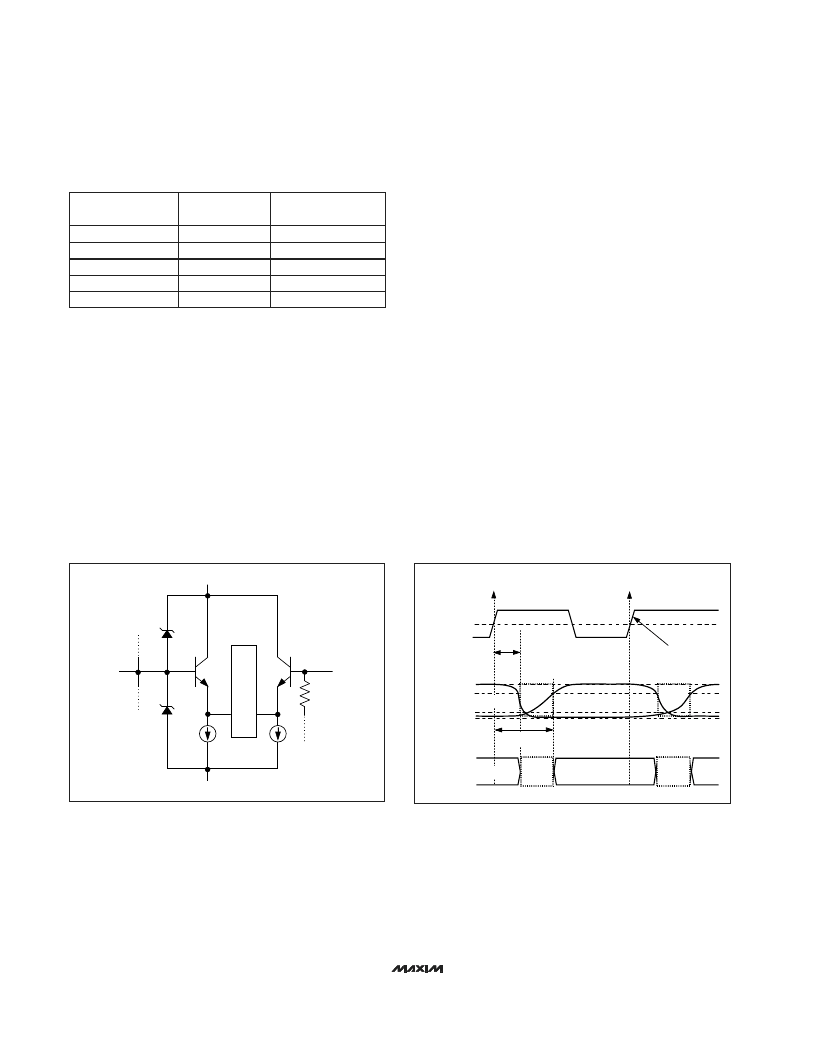
VIN
VFT
V
CC
V
EE
A
Figure 3. Analog Equivalent Input Circuit
Table 2. Output Data Information
CLK IN
DATA
OUT
(ACTUAL)
2.4V
3.5V
2.4V
0.5V
0.8V
t
pd1
typ
6ns
N
N + 1
DATA OUT
(EQUIVALENT)
(N - 1)
N
(N - 1)
N
t
6ns
(N - 2)
(N - 2)
14ns typ
INVALID
DATA
INVALID
DATA
INVALID
DATA
INVALID
DATA
Figure 4. Digital Output Characteristics
ANALOG
INPUT
> +2V + 1/2LSB
+2V - 1LSB
0V
-2V + 1LSB
< 2V
0
0
0
0
1
OVERRANGE
D10
OUTPUT CODE
D9–D0
1 1 1 1 1 1 1 1 1 1
1 1 1 1 1 1 1 1 1
0 0 0 0 0 0 0 0 0
0 0 0 0 0 0 0 0 0 0
(
indicates the flickering bit between logic 0 and 1.)
相關(guān)PDF資料 |
PDF描述 |
|---|---|
| MAX1160 | Low-Voltage Adjustable Precision Shunt Regulator 3-SOT-23 -40 to 85 |
| MAX1160ACWI | 10-Bit, 20Msps, TTL-Output ADC |
| MAX1160BCPI | 10-Bit, 20Msps, TTL-Output ADC |
| MAX1160BCWI | 10-Bit, 20Msps, TTL-Output ADC |
| MAX1168AEEG | Multichannel, 16-Bit, 200ksps Analog-to-Digital Converters |
相關(guān)代理商/技術(shù)參數(shù) |
參數(shù)描述 |
|---|---|
| MAX1160ACWI | 制造商:MAXIM 制造商全稱(chēng):Maxim Integrated Products 功能描述:10-Bit, 20Msps, TTL-Output ADC |
| MAX1160BCPI | 制造商:MAXIM 制造商全稱(chēng):Maxim Integrated Products 功能描述:10-Bit, 20Msps, TTL-Output ADC |
| MAX1160BCWI | 制造商:MAXIM 制造商全稱(chēng):Maxim Integrated Products 功能描述:10-Bit, 20Msps, TTL-Output ADC |
| MAX1161 | 制造商:MAXIM 制造商全稱(chēng):Maxim Integrated Products 功能描述:10-Bit, 40Msps, TTL-Output ADC |
| MAX11610 | 制造商:MAXIM 制造商全稱(chēng):Maxim Integrated Products 功能描述:2.7V to 3.6V and 4.5V to 5.5V, Low-Power, 4-/8-/12-Channel, 2-Wire Serial 10-Bit ADCs |
發(fā)布緊急采購(gòu),3分鐘左右您將得到回復(fù)。