- 您現(xiàn)在的位置:買賣IC網(wǎng) > PDF目錄383308 > MAX1005EEE (MAXIM INTEGRATED PRODUCTS INC) IF Undersampler PDF資料下載
參數(shù)資料
| 型號: | MAX1005EEE |
| 廠商: | MAXIM INTEGRATED PRODUCTS INC |
| 元件分類: | 模擬信號調理 |
| 英文描述: | IF Undersampler |
| 中文描述: | SPECIALTY ANALOG CIRCUIT, PDSO16 |
| 封裝: | 0.150 INCH, 0.025 INCH PITCH, QSOP-16 |
| 文件頁數(shù): | 7/8頁 |
| 文件大小: | 95K |
| 代理商: | MAX1005EEE |
Digital Interfac e
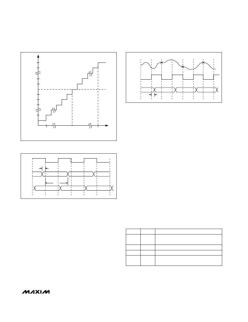
The DAC has a 7-bit parallel digital interface. Figure 2
shows the timing diagram for the transmit DAC. Digital
data is latched into the DAC input register on the falling
edge of CLK. On the next rising edge of CLK the data
is transferred to the DAC register and the DAC output
voltage is updated.
The ADC is enabled by setting TXEN = 0 and RXEN =
1. Figure 3 shows the ADC timing diagram. Input data
is sampled on the falling edge of CLK, while output
data changes state on the rising edge of CLK. This
minimizes digital feedthrough and noise while the ana-
log input is being sampled. The ADC output data is
applied to the 5-bit parallel output pins (D0–D4), with
the MSB at D4.
Operating Modes
The MAX1005 has three operating modes: transmit,
receive, and shutdown. The operating mode is selected
by the RXEN and TXEN inputs, as shown in Table 2.
In transmit mode, the DAC is active and the ADC is
inactive. Power consumption is typically 16.5mW with a
3V supply voltage. In receive mode, the ADC is active
and the DAC is inactive. Power consumption in this
mode is typically 39mW with a 3V supply voltage.
The third mode is shutdown, in which both the DAC
and the ADC are inactive. Select this mode by setting
RXEN = TXEN at any voltage from DGND to VCCD. In
shutdown mode, the CLK input can continue to run
without damaging the device and with no significant
increase in the typical shutdown supply current specifi-
cation of 0.1μA. When exiting shutdown, the MAX1005
is guaranteed to be operational within 2.4μs after TXEN
or RXEN is asserted, as shown in Table 2.
To prevent supply-current drain due to leakage cur-
rents from entering the ADC output bits, the ADC out-
puts (D0–D4) should not be held high in low-power
shutdown mode.
Table 2. Operating Mode Selection
M
IF Undersampler
_______________________________________________________________________________________
7
01111
01110
00010
00001
00000
11111
11110
11101
10001
10000
- FS
COM
INPUT VOLTAGE (LSB)
O
+FS
Figure 1. Receive ADC Transfer Function
CLK
DAC
OUTPUT
DAC
INPUT
DATA
(D0–D6)
n - 1
n
n + 1
n + 2
n - 1
n
n + 1
t
DS
t
HOLD
Figure 2. Transmit DAC Timing Diagram
ANALOG
INPUT
D0–D4
CLK
n - 1
n
SAMPLE
n
SAMPLE
n + 1
SAMPLE
n + 2
n + 1
t
DO
Figure 3. Receive ADC Timing Diagram
RXEN
TXEN
OPERATING MODE
0
0
Low-power shutdown: ADC and DAC
disabled
0
1
1
0
Transmit mode: DAC active, ADC disabled
Receive mode: ADC active, DAC disabled
1
1
Low-power shutdown: ADC and DAC
disabled
相關PDF資料 |
PDF描述 |
|---|---|
| MAX101 | 500Msps, 8-Bit ADC with Track/Hold |
| MAX101CFR | 500Msps, 8-Bit ADC with Track/Hold |
| MAX101A | 500Msps, 8-Bit ADC with Track/Hold |
| MAX1026ACEE-T | 10-Bit 300ksps ADCs with FIFO, Temp Sensor, Internal Reference |
| MAX1026AEEE-T | 10-Bit 300ksps ADCs with FIFO, Temp Sensor, Internal Reference |
相關代理商/技術參數(shù) |
參數(shù)描述 |
|---|---|
| MAX1005EEE+ | 功能描述:射頻無線雜項 IF Undersampler RoHS:否 制造商:Texas Instruments 工作頻率:112 kHz to 205 kHz 電源電壓-最大:3.6 V 電源電壓-最小:3 V 電源電流:8 mA 最大功率耗散: 工作溫度范圍:- 40 C to + 110 C 封裝 / 箱體:VQFN-48 封裝:Reel |
| MAX1005EEE+T | 功能描述:射頻無線雜項 IF Undersampler RoHS:否 制造商:Texas Instruments 工作頻率:112 kHz to 205 kHz 電源電壓-最大:3.6 V 電源電壓-最小:3 V 電源電流:8 mA 最大功率耗散: 工作溫度范圍:- 40 C to + 110 C 封裝 / 箱體:VQFN-48 封裝:Reel |
| MAX1005EEE-T | 功能描述:射頻無線雜項 RoHS:否 制造商:Texas Instruments 工作頻率:112 kHz to 205 kHz 電源電壓-最大:3.6 V 電源電壓-最小:3 V 電源電流:8 mA 最大功率耗散: 工作溫度范圍:- 40 C to + 110 C 封裝 / 箱體:VQFN-48 封裝:Reel |
| MAX1007 | 制造商:MAXIM 制造商全稱:Maxim Integrated Products 功能描述:Mobile-Radio Analog Controller |
| MAX1007CAG | 制造商:MAXIM 制造商全稱:Maxim Integrated Products 功能描述:Mobile-Radio Analog Controller |
發(fā)布緊急采購,3分鐘左右您將得到回復。