- 您現(xiàn)在的位置:買賣IC網(wǎng) > PDF目錄296459 > MADP-017015-13140G SILICON, PIN DIODE PDF資料下載
參數(shù)資料
| 型號(hào): | MADP-017015-13140G |
| 元件分類: | 參考電壓二極管 |
| 英文描述: | SILICON, PIN DIODE |
| 封裝: | ROHS COMLPLIANT, CASE ODS-1314, 2 PIN |
| 文件頁數(shù): | 1/4頁 |
| 文件大?。?/td> | 193K |
| 代理商: | MADP-017015-13140G |
North America Tel: 800.366.2266 / Fax: 978.366.2266
Europe Tel: 44.1908.574.200 / Fax: 44.1908.574.300
Asia/Pacific Tel: 81.44.844.8296 / Fax: 81.44.844.8298
Visit www.macom.com for additional data sheets and product information.
M/A-COM Inc. and its affiliates reserve the right to make changes to the product(s) or
information contained herein without notice.
SURMOUNT 15μM PIN Diodes
RoHS Compliant
M/A-COM Products
V4
MADP-017015-1314
MADP-030015-1314
ADVANCED:
Data Sheets contain information regarding a product M/A-COM is considering for
development. Performance is based on target specifications, simulated results, and/or prototype
measurements. Commitment to develop is not guaranteed.
PRELIMINARY:
Data Sheets contain information regarding a product M/A-COM has under develop-
ment. Performance is based on engineering tests. Specifications are typical. Mechanical outline has
been fixed. Engineering samples and/or test data may be available. Commitment to produce in
volume is not guaranteed.
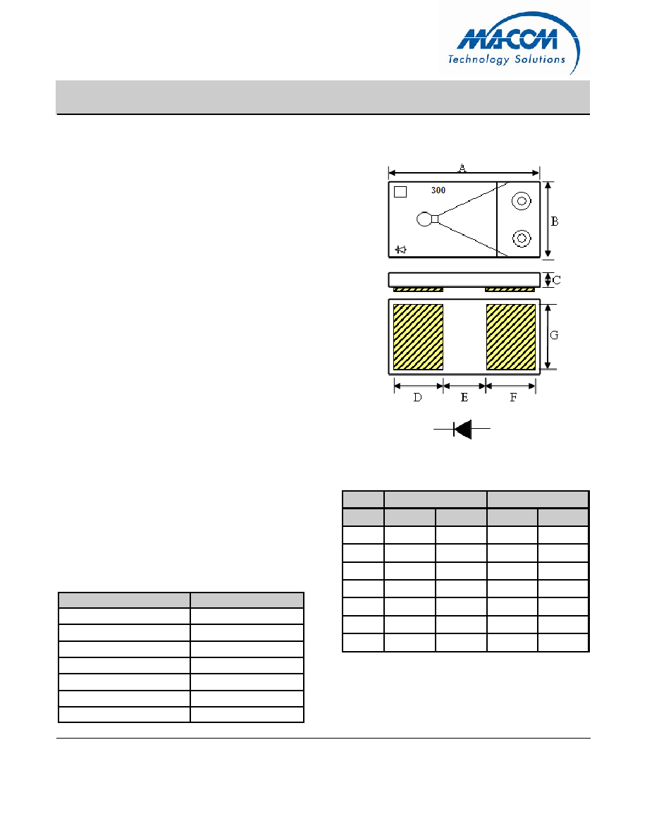
Case Style ODS 1314
Absolute Maximum Ratings
1 @T
AMB = +25°C
(unless otherwise specified)
1) Exceeding these limits may cause in permanent damage
Chip Dimensions
DIM
INCHES
MM
Min
Max
Min
Max
A
0.060
0.062
1.525
1.575
B
0.031
0.032
0.775
0.825
C
0.004
0.008
0.102
0.203
D
0.019
0.021
0.475
0.525
E
0.019
0.021
0.475
0.525
F
0.019
0.021
0.475
0.525
G
0.029
0.031
0.725
0.775
Notes:
1) Backside metal: 0.1microns thick.
2) Yellow area with hatch lines indicate backside ohmic gold
contacts.
3) Both devices have same outline dimensions ( A to G).
Features
0603 Outline
Surface Mount
15m I-Region Length Devices
No Wirebonds Required
Silicon Nitride Passivation
Polymer Scratch Protection
Low Parasitic Capacitance and Inductance
High Average and Peak Power Handling
Description
This device is a silicon, glass PIN diode surmount chip
fabricated with M/A-COM’s patented HMICTM process.
This device features two silicon pedestals embedded in a
low loss, low dispersion glass. The diode is formed on the
top of one pedestal and connections to the backside of the
device are facilitated by making the pedestal sidewalls
electrically conductive. Selective backside metallization is
applied producing a surface mount device. This vertical
topology provides for exceptional heat transfer. The
topside is fully encapsulated with silicon nitride and has an
additional polymer layer for scratch and impact protection.
These protective coatings prevent damage to the junction
and the anode air-bridge during handling and assembly.
Applications
These packageless devices are suitable for usage in
moderate incident power, ≤ 50dBm/C.W. or where the
peak power is ≤ 75dBm, pulse width is ≤ 1μS, and duty
cycle is ≤ 0.01%. Their low parasitic inductance, 0.4 nH,
and excellent RC constant, make these devices a superior
choice for higher frequency switch elements when
compared to their plastic package counterparts
.
Parameter
Absolute Maximum
Forward Current
500 mA
Reverse Voltage
- 115 V
Operating Temperature
-55°C to +125°C
Storage Temperature
-55 °C to +150°C
Junction Temperature
+175°C
C.W. Incident Power
50dBm
Mounting Temperature
+280°C for 30 seconds
相關(guān)PDF資料 |
PDF描述 |
|---|---|
| MADP-030015-13140G | SILICON, PIN DIODE |
| MADP-017025-13140G | SILICON, PIN DIODE |
| MADP00716101269 | SILICON, PIN DIODE |
| MADS-001317-1320AG | SILICON, mm WAVE BAND, MIXER DIODE |
| MAIA-007150-0001TR | RF/MICROWAVE MODULATOR |
相關(guān)代理商/技術(shù)參數(shù) |
參數(shù)描述 |
|---|---|
| MADP-017015-13140P | 功能描述:PIN 二極管 1-6000MHz .32pF -55C +125C RoHS:否 制造商:Skyworks Solutions, Inc. 配置: 反向電壓:200 V 正向連續(xù)電流: 頻率范圍:10 MHz to 6 GHz 端接類型:SMD/SMT 封裝 / 箱體:QFN-3 封裝:Reel |
| MADP-017025-1314 | 制造商:MA-COM 制造商全稱:M/A-COM Technology Solutions, Inc. 功能描述:SURMOUNT? 25μM PIN Diodes RoHS Compliant |
| MADP-017025-13140G | 制造商:M/A-COM Technology Solutions 功能描述:RF PIN DIODE |
| MADP-017025-13140P | 制造商:MA-COM 制造商全稱:M/A-COM Technology Solutions, Inc. 功能描述:SURMOUNT? 25μM PIN Diodes RoHS Compliant |
| MADP-017025-1314G | 制造商:M/A-COM Technology Solutions 功能描述:SURMOUNT- 25?M PIN DIODES - Gel-pak, waffle pack, wafer, diced wafer on film |
發(fā)布緊急采購,3分鐘左右您將得到回復(fù)。