- 您現(xiàn)在的位置:買賣IC網(wǎng) > PDF目錄45073 > MAC7122MAG50XX (FREESCALE SEMICONDUCTOR INC) MICROCONTROLLER, PQFP112 PDF資料下載
參數(shù)資料
第1頁第2頁第3頁第4頁第5頁第6頁第7頁第8頁第9頁第10頁第11頁第12頁第13頁當(dāng)前第14頁第15頁第16頁第17頁第18頁第19頁第20頁第21頁第22頁第23頁第24頁第25頁第26頁第27頁第28頁第29頁第30頁第31頁第32頁第33頁第34頁第35頁第36頁第37頁第38頁第39頁第40頁第41頁第42頁第43頁第44頁第45頁第46頁第47頁第48頁第49頁第50頁第51頁第52頁第53頁第54頁第55頁第56頁
ElectricalCharacteristics
MAC7100 Microcontroller Family Hardware Specifications, Rev. 1.2
Preliminary
Freescale Semiconductor
21
3.9.1
Read and Write Bus Cycles
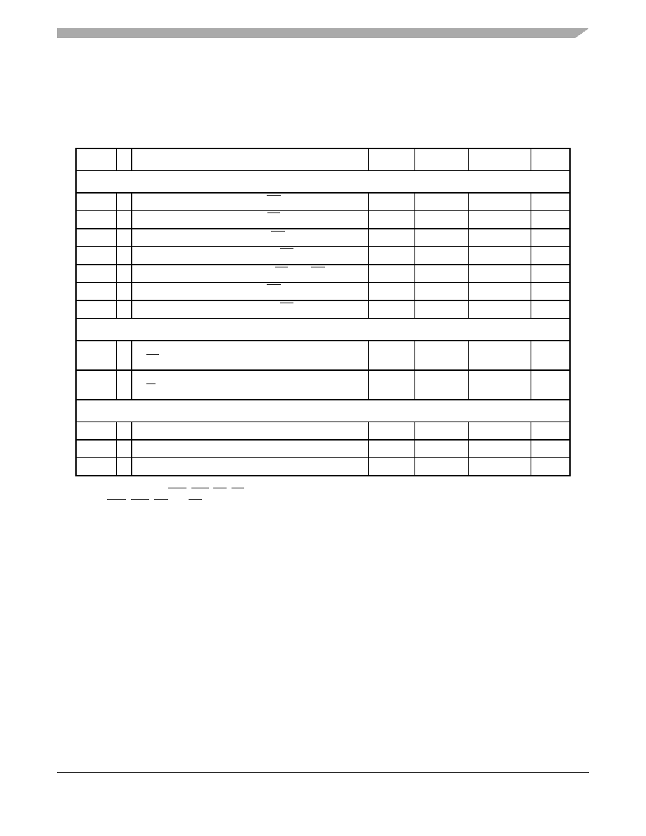
Table 25. External Bus Output Timing Specifications 1
NOTES:
1. Assumes CLKOUT, CSn, BSn, OE, AS, ADDR[21:0] and DATA[15:0] are configured for full drive strength (via the PIM).
Num
C
Rating
Symbol
Min
Max
Unit
Control Outputs
M6a
P CLKOUT high 2 to chip selects (CS[2:0]) valid
2. The CSn, BSn, OE and AS signals are synchronous to the falling edge of CLKOUT. Therefore, changes on these
signals are triggered by the falling edge of CLKOUT, even though they are specified in relation to the rising edge.
tCHCV
—0.5tCYC + 10
ns
M6b
P CLKOUT high 2 to byte selects (BS[1:0]) valid
tCHBV
—0.5tCYC + 10
ns
M6c
P CLKOUT high 2 to output select (OE) valid
tCHOV
—0.5tCYC + 10
ns
M6d
P CLKOUT high 2 to address strobe (AS) valid
tCHASV
—0.5tCYC + 10
ns
M7a
P CLKOUT high 2 to control output (BS[1:0], OE) invalid
tCHCOI
0.5tCYC + 2
—
ns
M7b
P CLKOUT high 2 to chip selects (CS[2:0]) invalid
tCHCI
0.5tCYC + 2
—
ns
M7c
P CLKOUT high 2 to address strobe (AS) invalid
tCHASI
0.5tCYC + 2
—
ns
Address and Attribute Outputs
M8
P CLKOUT high to address (ADDR[21:0]) and control
(R/W) valid
tCHAV
—10
ns
M9
P CLKOUT high to address (ADDR[21:0]) and control
(R/W) invalid
tCHAI
2—
ns
Data Outputs
M10
P CLKOUT high to data output (DATA[15:0]) valid
tCHDOV
—13
ns
M11
P CLKOUT high to data output (DATA[15:0]) invalid
tCHDOI
2—
ns
M12
D CLKOUT high to data output (DATA[15:0]) high impedance
tCHDOZ
—9
ns
Because
of
an
order
from
the
United
States
International
Trade
Commission,
BGA-packaged
product
lines
and
part
numbers
indicated
here
currently
are
not
available
from
Freescale
for
import
or
sale
in
the
United
States
prior
to
September
2010:MAC7131
products
in
208
MAPBGA
packages
相關(guān)PDF資料 |
PDF描述 |
|---|---|
| MAC7126MPV50XX | MICROCONTROLLER, PQFP112 |
| MAC7142CAF50XX | MICROCONTROLLER, PQFP100 |
| MAC7142CFU50XX | MICROCONTROLLER, PQFP100 |
| MAC7121VPV50XX | MICROCONTROLLER, PQFP112 |
| MAC7122VAG50XX | MICROCONTROLLER, PQFP112 |
相關(guān)代理商/技術(shù)參數(shù) |
參數(shù)描述 |
|---|---|
| MAC7122MFU50 | 制造商:FREESCALE 制造商全稱:Freescale Semiconductor, Inc 功能描述:Microcontroller Family Hardware Specifications |
| MAC7122MPV50 | 制造商:FREESCALE 制造商全稱:Freescale Semiconductor, Inc 功能描述:Microcontroller Family Hardware Specifications |
| MAC7122MVF50 | 制造商:FREESCALE 制造商全稱:Freescale Semiconductor, Inc 功能描述:Microcontroller Family Hardware Specifications |
| MAC7122MVM50 | 制造商:FREESCALE 制造商全稱:Freescale Semiconductor, Inc 功能描述:Microcontroller Family Hardware Specifications |
| MAC7122VAF50 | 制造商:FREESCALE 制造商全稱:Freescale Semiconductor, Inc 功能描述:Microcontroller Family Hardware Specifications |
發(fā)布緊急采購,3分鐘左右您將得到回復(fù)。