- 您現(xiàn)在的位置:買(mǎi)賣(mài)IC網(wǎng) > PDF目錄358129 > MA05130-DIE VCO, 2150 MHz - 2350 MHz PDF資料下載
參數(shù)資料
| 型號(hào): | MA05130-DIE |
| 元件分類: | XO, clock |
| 英文描述: | VCO, 2150 MHz - 2350 MHz |
| 文件頁(yè)數(shù): | 2/4頁(yè) |
| 文件大小: | 63K |
| 代理商: | MA05130-DIE |

S-Band Voltage Controlled Oscillator
MA05130-DIE
V 1P.00
M/A-COM Inc. and its affiliates reserve the right to make changes to the product(s)
or information contained herein without notice. M/A-COM makes no warranty,
representation, or guarantee regarding the suitability of its products for any particular
purpose, nor does M/A-COM assume any liability whatsoever arising out of the use
or application of any product(s) or information.
Visit www.macom.com for additional data sheets and product information.
n
North America:
Tel. (978) 656-2693
n
Asia/Pacific:
Tel.+81-44-844-8296, Fax +81-44-844-8298
n
Europe:
Tel. +44 (1344) 869 595, Fax+44 (1344) 300 020
2
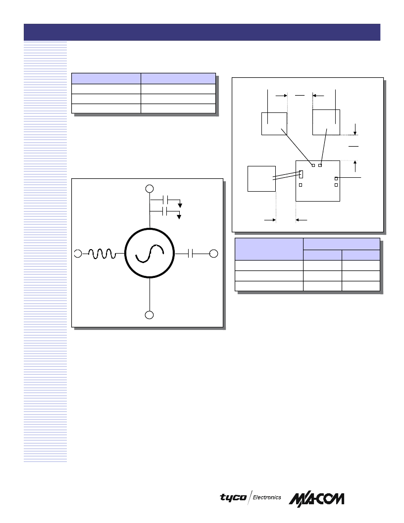
Recommended Bare Die Configuration
5,6,7,8
Absolute Maximum Ratings
1,2
1.
Exceeding any one or a combination of these limits may
cause permanent damage.
Adequate DC and RF grounding required on board.
2.
Parameter
Absolute Maximum
V
CC
+ 5 V
Operating Temperature
-40°C to +85°C
Storage Temperature
-65°C to +150°C
Component Nominal Value
Nominal Value
Lower S-Band Upper S-Band
Inductor, L1
2.5 nH
2.25 nH
Tuning Capacitor, C1
0.5 pF
0.5 pF
100 pF
100 pF
Capacitor, C2
C1
U1
C2
L1
0.017
0.43
0.021
0.43
0.020
0.51
OUT
V
CC
TUNE
5.
The position of the inductor and the bond wire lengths
are critical in determining the frequency band.
For inductor, L1, it is recommend using M/A-COM’s
1000004710.
The value of the tuning capacitor determines the fre-
quency range.
The die requires sufficient backside grounding using
either conductive epoxy or solder.
6.
7.
8.
Recommended Bias Configuration
3,4
3.
For optimum performance, V
bypass capacitors should
be placed within 0.5 inches of the V
leads.
For optimum performance, V
inductor should be placed
within 0.3 inches of the V
tune
leads.
4.
FE55-0005
RF Out
6
Tune
2
GND
1,4,5,8
100 pF
V
cc
7
100nH
10 pF
100nF
相關(guān)PDF資料 |
PDF描述 |
|---|---|
| MA05423 | TCXO, SINE OUTPUT, 16.367667 MHz |
| MA05630 | VCO, 1230 MHz - 1290 MHz |
| MA09355 | 1-PORT SAW RESONATOR, 1000 MHz |
| MA141K | SILICON, MIXER DIODE |
| MA151WK | SILICON, MIXER DIODE |
相關(guān)代理商/技術(shù)參數(shù) |
參數(shù)描述 |
|---|---|
| MA0515XD-1W | 制造商:MICRODC 制造商全稱:MICRODC 功能描述:1W/2W, FIXED INPUT , ISOLA TED & REGULATED DUAL OUTPUT DC-DC CONVERTER |
| MA0515XD-3W | 制造商:MICRODC 制造商全稱:MICRODC 功能描述:1000VDC Isolated 3WDual&single output DIP24 Converters |
| MA0520N2510A | 制造商:AAC 制造商全稱:American Accurate Components, Inc. 功能描述:Broadband Limiting Amplifiers 0.5 to 18GHz |
| MA0520N2510B | 制造商:AAC 制造商全稱:American Accurate Components, Inc. 功能描述:Broadband Limiting Amplifiers 0.5 to 18GHz |
| MA0520N3005A | 制造商:AAC 制造商全稱:American Accurate Components, Inc. 功能描述:Broadband Limiting Amplifiers 0.5 to 18GHz |
發(fā)布緊急采購(gòu),3分鐘左右您將得到回復(fù)。