- 您現(xiàn)在的位置:買賣IC網(wǎng) > PDF目錄45053 > M906-01I125.2500 (INTEGRATED DEVICE TECHNOLOGY INC) 125 MHz, OTHER CLOCK GENERATOR, CQCC36 PDF資料下載
參數(shù)資料
| 型號: | M906-01I125.2500 |
| 廠商: | INTEGRATED DEVICE TECHNOLOGY INC |
| 元件分類: | 時鐘產(chǎn)生/分配 |
| 英文描述: | 125 MHz, OTHER CLOCK GENERATOR, CQCC36 |
| 封裝: | 9 X 9 MM, CERAMIC, LCC-36 |
| 文件頁數(shù): | 3/6頁 |
| 文件大?。?/td> | 282K |
| 代理商: | M906-01I125.2500 |
M906-01 Datasheet Rev 1.3
3 of 6
Revised 06Jan2004
Integ r ated Circuit Systems , Inc. ● Comm unications Modules ● www.i cst. com ● tel (508) 852-5400
M906-01
VCSO BASED GBE CLOCK GENERATOR
Preliminar y In f o r m atio n
FUNCTIONAL DESCRIPTION
The M906-01 is a PLL (Phase Locked Loop) based
clock generator that generates output clocks
synchronized to an input reference clock.
The M906-01 combines the flexibility of a VCSO
(Voltage Controlled SAW Oscillator) with the stability of
a crystal oscillator.
Input Reference
The input reference can either be an external, discrete
crystal device or a stable external clock source such as
a packaged crystal oscillator:
If an external crystal is used with the on-chip crystal
oscillator circuit (XTAL OSC), the external crystal
should be a parallel-resonant, fundamental mode
crystal. Apply it to the XTAL_1 / REF_IN and XTAL_2 input
pins. External crystal load capacitors are also
required.
If an external LVCMOS/LVTTL clock source is used,
apply it to the XTAL_1 / REF_IN input pin.
In either case, the reference clock is supplied to the
phase detector of the PLL. The M906-01 includes a
reference divider that divides the input reference
frequency by a fixed value “R” and provides the result to
the phase detector.
The EX_CLK pin is available for a clock feed-through
mode for testing. See “External Clock Feed-through”
on pg. 4.
The PLL
The PLL (Phase Locked Loop) includes the phase
detector, the VCSO, a feedback divider (labeled
“M Divider”), and a reference divider (“R Divider”).
The feedback divider divides the VCSO output
frequency by a fixed value “M” to match the reference
frequency provided to the phase detector by the
reference divider.
By controlling the frequency and phase of the VCSO,
the phase detector precisely locks the frequency and
phase of the feedback divider output to that of the
reference divider output. This creates an output
frequency that is a multiple of the reference frequency
(which is output from the VCSO).
The relationship between the VCSO output frequency,
the M Divider, the R Divider and the input reference
frequency is defined as follows:
For the M906-01-156.2500 (see “Ordering Information” on pg. 6):
VCSO output frequency = 156.25MHz
Input reference frequency = 25MHz
M=25
R= 4
Therefore, for the M906-01-156.2500:
25
156.25MHz = 25MHz
4
The product of the input crystal frequency and
falls within the lock range of the VCSO.
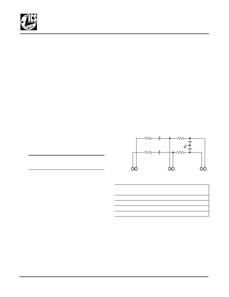
External Loop Filter
To provide stable PLL operation, and thereby a low jitter
output clock, the M906-01 requires the use of an
external loop filter. This is provided via the provided
filter pins (see Figure 4).
Due to the differential signal path design, the
implementation requires two identical complementary
RC filters as shown here.
Figure 4: External Loop Filter
Fvcso
Fxtal
M
R
-----
×
=
External Loop Filter Component Values
PLL
Bandwidth
Damping
Factor
R loop
C loop R post C post
500
Hz
2.1
1.5
k
4.00F 50k 3300pF
1.5
kHz
3.3
4.7
k
1.00F 50k 1500pF
6.4
kHz
4.4
20.0
k
0.10F 20k
470
pF
10.6
kHz 1
Note 1: Recommended for most applications
4.2
33.0
k
0.033F 20k
470
pF
----------
×
M
R
-----
C
POST
C
POST
VC
nVC
R
POST
nOP_OUT
OP_OUT
R
POST
R
LOOP
R
LOOP
C
LOOP
C
LOOP
OP_IN
nOP_IN
相關(guān)PDF資料 |
PDF描述 |
|---|---|
| M906-01-125.2500 | 125 MHz, OTHER CLOCK GENERATOR, CQCC36 |
| M906-02I175.0000 | 175 MHz, OTHER CLOCK GENERATOR, CQCC36 |
| M906-02-155.5200LF | 155.52 MHz, OTHER CLOCK GENERATOR, CQCC36 |
| M906-02-150.0000 | 150 MHz, OTHER CLOCK GENERATOR, CQCC36 |
| M906-02I150.0000 | 150 MHz, OTHER CLOCK GENERATOR, CQCC36 |
相關(guān)代理商/技術(shù)參數(shù) |
參數(shù)描述 |
|---|---|
| M906-01I156.2500 | 功能描述:時鐘發(fā)生器及支持產(chǎn)品 SAW CLOCK GENERATOR RoHS:否 制造商:Silicon Labs 類型:Clock Generators 最大輸入頻率:14.318 MHz 最大輸出頻率:166 MHz 輸出端數(shù)量:16 占空比 - 最大:55 % 工作電源電壓:3.3 V 工作電源電流:1 mA 最大工作溫度:+ 85 C 安裝風(fēng)格:SMD/SMT 封裝 / 箱體:QFN-56 |
| M906-01I156.2500T | 制造商:Integrated Device Technology Inc 功能描述:SAW CLOCK GENERATOR 制造商:Integrated Device Technology Inc 功能描述:9X9 LCC(LEAD FREE) - Tape and Reel |
| M906-01I187.5000 | 制造商:ICS 制造商全稱:ICS 功能描述:VCSO BASED GBE CLOCK GENERATOR |
| M90-6020845 | 制造商:Harwin 功能描述: |
| M90-604 | 制造商:HARWIN 制造商全稱:Harwin Plc 功能描述:SPRING PROBE ASSEMBLY LONG TAIL |
發(fā)布緊急采購,3分鐘左右您將得到回復(fù)。