- 您現(xiàn)在的位置:買賣IC網(wǎng) > PDF目錄4437 > M7A3P1000-FG144I (Microsemi SoC)IC FPGA 1KB FLASH 1M 144-FBGA PDF資料下載
參數(shù)資料
| 型號: | M7A3P1000-FG144I |
| 廠商: | Microsemi SoC |
| 文件頁數(shù): | 170/220頁 |
| 文件大小: | 0K |
| 描述: | IC FPGA 1KB FLASH 1M 144-FBGA |
| 標準包裝: | 160 |
| 系列: | ProASIC3 |
| RAM 位總計: | 147456 |
| 輸入/輸出數(shù): | 97 |
| 門數(shù): | 1000000 |
| 電源電壓: | 1.425 V ~ 1.575 V |
| 安裝類型: | 表面貼裝 |
| 工作溫度: | -40°C ~ 85°C |
| 封裝/外殼: | 144-LBGA |
| 供應商設備封裝: | 144-FPBGA(13x13) |
第1頁第2頁第3頁第4頁第5頁第6頁第7頁第8頁第9頁第10頁第11頁第12頁第13頁第14頁第15頁第16頁第17頁第18頁第19頁第20頁第21頁第22頁第23頁第24頁第25頁第26頁第27頁第28頁第29頁第30頁第31頁第32頁第33頁第34頁第35頁第36頁第37頁第38頁第39頁第40頁第41頁第42頁第43頁第44頁第45頁第46頁第47頁第48頁第49頁第50頁第51頁第52頁第53頁第54頁第55頁第56頁第57頁第58頁第59頁第60頁第61頁第62頁第63頁第64頁第65頁第66頁第67頁第68頁第69頁第70頁第71頁第72頁第73頁第74頁第75頁第76頁第77頁第78頁第79頁第80頁第81頁第82頁第83頁第84頁第85頁第86頁第87頁第88頁第89頁第90頁第91頁第92頁第93頁第94頁第95頁第96頁第97頁第98頁第99頁第100頁第101頁第102頁第103頁第104頁第105頁第106頁第107頁第108頁第109頁第110頁第111頁第112頁第113頁第114頁第115頁第116頁第117頁第118頁第119頁第120頁第121頁第122頁第123頁第124頁第125頁第126頁第127頁第128頁第129頁第130頁第131頁第132頁第133頁第134頁第135頁第136頁第137頁第138頁第139頁第140頁第141頁第142頁第143頁第144頁第145頁第146頁第147頁第148頁第149頁第150頁第151頁第152頁第153頁第154頁第155頁第156頁第157頁第158頁第159頁第160頁第161頁第162頁第163頁第164頁第165頁第166頁第167頁第168頁第169頁當前第170頁第171頁第172頁第173頁第174頁第175頁第176頁第177頁第178頁第179頁第180頁第181頁第182頁第183頁第184頁第185頁第186頁第187頁第188頁第189頁第190頁第191頁第192頁第193頁第194頁第195頁第196頁第197頁第198頁第199頁第200頁第201頁第202頁第203頁第204頁第205頁第206頁第207頁第208頁第209頁第210頁第211頁第212頁第213頁第214頁第215頁第216頁第217頁第218頁第219頁第220頁
ProASIC3 Flash Family FPGAs
Revision 13
2-39
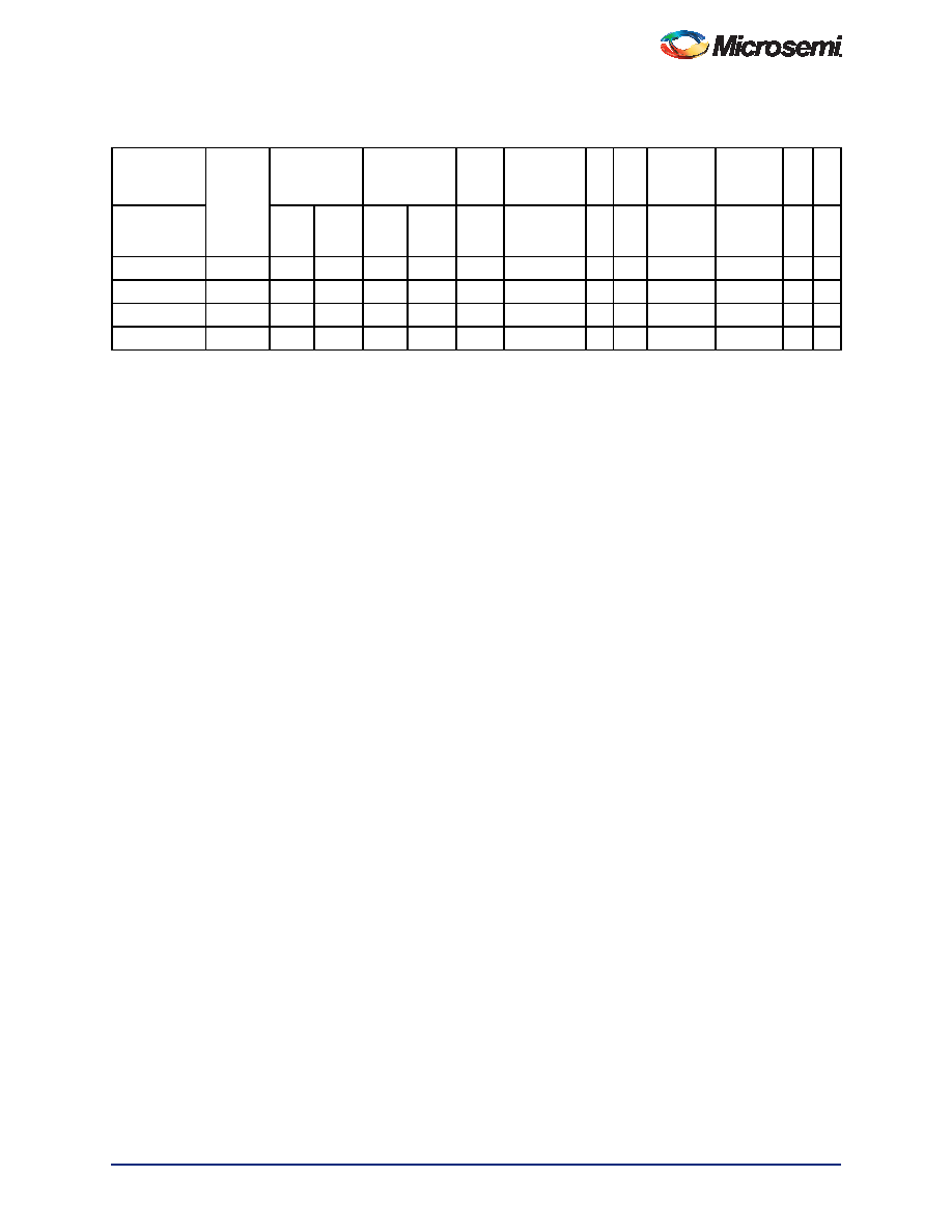
Table 2-49 Minimum and Maximum DC Input and Output Levels
Applicable to Standard I/O Banks
3.3 V
LVCMOS
Wide Range
Equiv.
Software
Default
Drive
Strength
Option1
VIL
VIH
VOL
VOH
IOL IOH
IOSL
IOSH
IIL2 IIH3
Drive
Strength
Min.
V
Max.
V
Min.
V
Max.
V
Max.
V
Min.
VA A
Max.
mA4
Max.
mA4
A5 A5
100 A
2 mA
–0.3
0.8
2
3.6
0.2
VDD – 0.2 100 100
25
27
10 10
100 A
4 mA
–0.3
0.8
2
3.6
0.2
VDD – 0.2 100 100
25
27
10 10
100 A
6 mA
–0.3
0.8
2
3.6
0.2
VDD – 0.2 100 100
51
54
10 10
100 A
8 mA
–0.3
0.8
2
3.6
0.2
VDD – 0.2 100 100
51
54
10 10
Notes:
1. The minimum drive strength for any LVCMOS 3.3 V software configuration when run in wide range is ±100 A. Drive
strength displayed in the software is supported for normal range only. For a detailed I/V curve, refer to the IBIS models.
2. IIL is the input leakage current per I/O pin over recommended operation conditions where –0.3 V < VIN < VIL.
3. IIH is the input leakage current per I/O pin over recommended operating conditions VIH < VIN < VCCI. Input current is
larger when operating outside recommended ranges
4. Currents are measured at 85°C junction temperature.
5. All LVMCOS 3.3 V software macros support LVCMOS 3.3 V wide range as specified in the JESD8-B specification.
6. Software default selection highlighted in gray.
相關PDF資料 |
PDF描述 |
|---|---|
| M7A3P1000-FGG144I | IC FPGA 1KB FLASH 1M 144-FBGA |
| EPF10K30EQI208-2N | IC FLEX 10KE FPGA 30K 208-PQFP |
| EPF10K30EQI208-2 | IC FLEX 10KE FPGA 30K 208-PQFP |
| EP20K100EQC208-2XN | IC APEX 20KE FPGA 100K 208-PQFP |
| 8655MHRA2501LF | BACKSHELL DB25 45DEG METAL SHLD |
相關代理商/技術參數(shù) |
參數(shù)描述 |
|---|---|
| M7A3P1000-FG256 | 功能描述:IC FPGA 1KB FLASH 1M 256-FBGA RoHS:否 類別:集成電路 (IC) >> 嵌入式 - FPGA(現(xiàn)場可編程門陣列) 系列:ProASIC3 標準包裝:40 系列:SX-A LAB/CLB數(shù):6036 邏輯元件/單元數(shù):- RAM 位總計:- 輸入/輸出數(shù):360 門數(shù):108000 電源電壓:2.25 V ~ 5.25 V 安裝類型:表面貼裝 工作溫度:0°C ~ 70°C 封裝/外殼:484-BGA 供應商設備封裝:484-FPBGA(27X27) |
| M7A3P1000-FG256I | 功能描述:IC FPGA 1KB FLASH 1M 256-FBGA RoHS:否 類別:集成電路 (IC) >> 嵌入式 - FPGA(現(xiàn)場可編程門陣列) 系列:ProASIC3 標準包裝:40 系列:SX-A LAB/CLB數(shù):6036 邏輯元件/單元數(shù):- RAM 位總計:- 輸入/輸出數(shù):360 門數(shù):108000 電源電壓:2.25 V ~ 5.25 V 安裝類型:表面貼裝 工作溫度:0°C ~ 70°C 封裝/外殼:484-BGA 供應商設備封裝:484-FPBGA(27X27) |
| M7A3P1000-FG484 | 功能描述:IC FPGA 1KB FLASH 1M 484-FBGA RoHS:否 類別:集成電路 (IC) >> 嵌入式 - FPGA(現(xiàn)場可編程門陣列) 系列:ProASIC3 標準包裝:40 系列:SX-A LAB/CLB數(shù):6036 邏輯元件/單元數(shù):- RAM 位總計:- 輸入/輸出數(shù):360 門數(shù):108000 電源電壓:2.25 V ~ 5.25 V 安裝類型:表面貼裝 工作溫度:0°C ~ 70°C 封裝/外殼:484-BGA 供應商設備封裝:484-FPBGA(27X27) |
| M7A3P1000-FG484I | 功能描述:IC FPGA 1KB FLASH 1M 484-FBGA RoHS:否 類別:集成電路 (IC) >> 嵌入式 - FPGA(現(xiàn)場可編程門陣列) 系列:ProASIC3 產(chǎn)品培訓模塊:Three Reasons to Use FPGA's in Industrial Designs Cyclone IV FPGA Family Overview 特色產(chǎn)品:Cyclone? IV FPGAs 標準包裝:60 系列:CYCLONE® IV GX LAB/CLB數(shù):9360 邏輯元件/單元數(shù):149760 RAM 位總計:6635520 輸入/輸出數(shù):270 門數(shù):- 電源電壓:1.16 V ~ 1.24 V 安裝類型:表面貼裝 工作溫度:0°C ~ 85°C 封裝/外殼:484-BGA 供應商設備封裝:484-FBGA(23x23) |
| M7A3P1000-FGG144 | 功能描述:IC FPGA 1KB FLASH 1M 144-FBGA RoHS:是 類別:集成電路 (IC) >> 嵌入式 - FPGA(現(xiàn)場可編程門陣列) 系列:ProASIC3 標準包裝:40 系列:SX-A LAB/CLB數(shù):6036 邏輯元件/單元數(shù):- RAM 位總計:- 輸入/輸出數(shù):360 門數(shù):108000 電源電壓:2.25 V ~ 5.25 V 安裝類型:表面貼裝 工作溫度:0°C ~ 70°C 封裝/外殼:484-BGA 供應商設備封裝:484-FPBGA(27X27) |
發(fā)布緊急采購,3分鐘左右您將得到回復。