- 您現(xiàn)在的位置:買賣IC網 > PDF目錄370992 > M66515 (Mitsubishi Electric Corporation) LASER-DIODE DRIVER/CONTROLLER PDF資料下載
參數(shù)資料
| 型號: | M66515 |
| 廠商: | Mitsubishi Electric Corporation |
| 英文描述: | LASER-DIODE DRIVER/CONTROLLER |
| 中文描述: | 激光二極管驅動器/控制器 |
| 文件頁數(shù): | 5/7頁 |
| 文件大?。?/td> | 174K |
| 代理商: | M66515 |
5
MITSUBISHI
DIGITAL ASSP
M66515FP
LASER-DIODE DRIVER/CONTROLLER
Min.
4.75
–20
Typ.
5.0
Max.
5.25
120
30
70
Unit
V
mA
mA
°
C
Parameter
Supply voltage
Switing current
Bias current
Operating ambient temperature
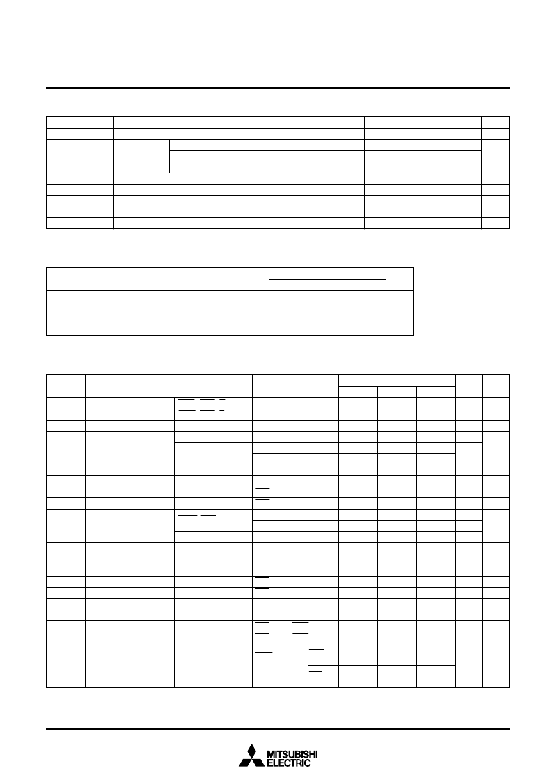
RECOMMENDED OPERATIONAL CONDITIONS
(T
a
= –20 ~ 70
°
C unless otherwise noted)
Ratings
–0.5 ~ +7.0
–0.3 ~ V
CC
–0.3 ~ +7.0
–0.3 ~ +7.0
150
45
1200
–65 ~ 150
Parameter
Supply voltage
Input voltage
Output voltage
Switching current
Bias current
Power dissipation
Storage temperature
Symbol
V
CC
V
I
V
O
I
SW
I
B
P
d
T
stg
Unit
V
V
V
mA
mA
mW
°
C
ABSOLUTE MAXIMUM RATINGS
(T
a
= –20 ~ 70
°
C unless otherwise noted)
Conditions
Measured being mounted
Ta = 25
°
C
C
H
, V
r
DATE, ENB, S/H
RO
Symbol
V
CC
I
SW
I
B
T
opr
Limits
Max.
0.8
2.0
V
CC
0.6
20
–0.2
±
1
–2.0
2.0
±
5
50
50
75
74
Test
circuit
“H” Input voltage
“L” Input voltage
Reference voltage input
Reference voltage
output
Operating voltage range
Maximum effective voltage
“H” output voltage
“L” output voltage
Input current
Switching current (Note)
Bias current
Load charging current
Load discharging current
(Note)
Test conditions
I
O
= –10
μ
A
T
a
=
–
20 ~ 25
°
C
T
a
= 20 ~ 70
°
C
ENB = 0.8V, I
OH
= –2mA
ENB = 0.8V, I
OL
= 2mA
V
I
= 2.7V
V
I
= 0.4V
V
I
= 0 ~ V
CC
C
H
= 3.0V, R
S
= 300
, V
LD
= 2V
T
a
= 20 ~ 70
°
C
V
B
= 1.2V, R
B
= 360
, V
LD
= 2V
ENB = 0.8V, V
O
= 0.6 ~ 4.0V
ENB = 0.8V, V
O
= 0.6 ~ 4.0V
V
O
= 0 ~ V
CC
, Hold condition
ENB = 0.8V, DATA = 2.0V
ENB = 2.0V, DATA = 0.8V
V
CC
= 5.25V,
ENB = 0V,
C
H
= 3.0V, VB = 1.2V,
R
S
= 300
, R
B
= 360
,
RO = LD = 5.0V
Min.
2.0
0.4
2.5
V
CC
– 1.8
4.0
–0.66
0.66
Limits
Typ.
Symbol
V
IH
V
IL
V
r
V
ref
V
LD
V
I
V
OH
V
OL
I
I
I
SW
I
B
I
cg
I
dg
I
oz
I
OFF
I
CC
ELECTRICAL CHARACTERISTICS
(T
a
= –20 ~ 70
°
C, V
CC
= 5V
±
5% unless otherwise noted)
Unit
V
V
V
V
mV/
°
C
V
V
V
V
μ
A
mA
μ
A
mA
mA/
°
C
mA
mA
mA
μ
A
μ
A
mA
DATA, ENB, S/H
DATA, ENB, S/H
V
r
V
ref
Temprature
coefficient
LD
C
H
C
H
C
H
DATA, ENB
C
H
LD
LD
C
H
C
H
C
H
LD
Parameter
Temprature coefficient
DATA = 0V
DATA = 4.5V
1.2
–0.9
–0.9
V
CC
– 1.4
120
0.11
30
0.03
0.01
54
52
1
1
1
2
2
3
3
3
2
4
Typical values are gained under conditions of Ta = 25
°
C and Vcc = 5V.
Note: This parameter indicates the conversion characteristics of the input voltage and output current. In actual use, I
SW
and I
B
shall be within the range specified
as limits in the recommended operating conditions.
Output current under off
condition
Supply current
Output current under off
condition
相關PDF資料 |
PDF描述 |
|---|---|
| M66700P | DUAL HIGH-SPEED CCD CLOCK DRIVER |
| M66700WP | DUAL HIGH-SPEED CCD CLOCK DRIVER |
| M66701P | DUAL HIGH-SPEED CCD CLOCK DRIVER |
| M66851FP | SRAM TYPE FIFO MEMORY |
| M66850FP | SRAM TYPE FIFO MEMORY |
相關代理商/技術參數(shù) |
參數(shù)描述 |
|---|---|
| M66515FP | 制造商:MITSUBISHI 制造商全稱:Mitsubishi Electric Semiconductor 功能描述:LASER-DIODE DRIVER/CONTROLLER |
| M66515FP#TC2J | 功能描述:IC LASR CTRLR 40MBPS 5.25V 20SOP RoHS:是 類別:集成電路 (IC) >> PMIC - 激光驅動器 系列:- 產品培訓模塊:Lead (SnPb) Finish for COTS Obsolescence Mitigation Program 標準包裝:60 系列:- 類型:激光二極管驅動器 數(shù)據速率:- 通道數(shù):4 電源電壓:3.3V 電流 - 電源:- 電流 - 調制:- 電流 - 偏置:- 工作溫度:0°C ~ 70°C 封裝/外殼:40-TQFN 裸露焊盤 供應商設備封裝:40-TQFN EP 包裝:托盤 安裝類型:表面貼裝 |
| M66515FP(#TC2J) | 制造商:Renesas Electronics Corporation 功能描述: |
| M66516FP | 制造商:MITSUBISHI 制造商全稱:Mitsubishi Electric Semiconductor 功能描述:LASER-DIODE DRIVER/CONTROLLER |
| M6657 | 制造商:Tamura Corporation of America 功能描述: |
發(fā)布緊急采購,3分鐘左右您將得到回復。