- 您現(xiàn)在的位置:買賣IC網(wǎng) > PDF目錄359722 > M38B53EFXXXFS (Renesas Technology Corp.) SINGLE-CHIP 8-BIT CMOS MICROCOMPUTER PDF資料下載
參數(shù)資料
| 型號: | M38B53EFXXXFS |
| 廠商: | Renesas Technology Corp. |
| 英文描述: | SINGLE-CHIP 8-BIT CMOS MICROCOMPUTER |
| 中文描述: | 單芯片8位CMOS微機 |
| 文件頁數(shù): | 47/70頁 |
| 文件大小: | 864K |
| 代理商: | M38B53EFXXXFS |
第1頁第2頁第3頁第4頁第5頁第6頁第7頁第8頁第9頁第10頁第11頁第12頁第13頁第14頁第15頁第16頁第17頁第18頁第19頁第20頁第21頁第22頁第23頁第24頁第25頁第26頁第27頁第28頁第29頁第30頁第31頁第32頁第33頁第34頁第35頁第36頁第37頁第38頁第39頁第40頁第41頁第42頁第43頁第44頁第45頁第46頁當前第47頁第48頁第49頁第50頁第51頁第52頁第53頁第54頁第55頁第56頁第57頁第58頁第59頁第60頁第61頁第62頁第63頁第64頁第65頁第66頁第67頁第68頁第69頁第70頁
MITSUBISHI MICROCOMPUTERS
38B5 Group
SINGLE-CHIP 8-BIT CMOS MICROCOMPUTER
46
PRELIMINARY
Notice: This s not a final specification.
Some parametric imits are subject to change.
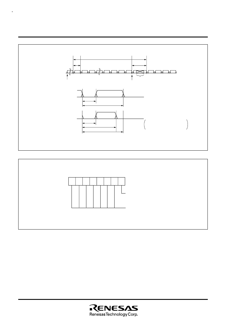
Fig. 50 Structure of P8FLD Output Control Register
Fig. 49 FLDC Timing
P8FLD output control register
(P8FLDCON: address 0EFC
16
)
P8
4
–P8
7
FLD output reverse bits
0: Output normally
1: Reverse output
Not available (returns “0” when read)
b7
b0
Toff1
Tdisp
Segment
Digit
Segment
Digit output
Segment setting by software
FLD blanking interrupt request occurs
at the falling edge of the last timing.
FLD digit interrupt request occurs at the rising
edge of digit (each timing).
Tdisp
Tscan
Repeat synchronous
Tn
Tn-1 Tn-2
T4
T3
T2
T1
Toff1
Toff2
Tdisp
Segment
Digit
When a gradation display mode is selected
Pin under the condition that bit 5 of the
FLDC mode register is “1,” and the
corresponding gradation display control
data value is “1.”
n: Number of timing
發(fā)布緊急采購,3分鐘左右您將得到回復(fù)。