- 您現(xiàn)在的位置:買賣IC網(wǎng) > PDF目錄299433 > M38B48E1H-XXXXFP (Mitsubishi Electric Corporation) SINGLE-CHIP 8-BIT CMOS MICROCOMPUTER PDF資料下載
參數(shù)資料
| 型號: | M38B48E1H-XXXXFP |
| 廠商: | Mitsubishi Electric Corporation |
| 英文描述: | SINGLE-CHIP 8-BIT CMOS MICROCOMPUTER |
| 中文描述: | 單芯片8位CMOS微機 |
| 文件頁數(shù): | 31/78頁 |
| 文件大?。?/td> | 1214K |
| 代理商: | M38B48E1H-XXXXFP |
第1頁第2頁第3頁第4頁第5頁第6頁第7頁第8頁第9頁第10頁第11頁第12頁第13頁第14頁第15頁第16頁第17頁第18頁第19頁第20頁第21頁第22頁第23頁第24頁第25頁第26頁第27頁第28頁第29頁第30頁當前第31頁第32頁第33頁第34頁第35頁第36頁第37頁第38頁第39頁第40頁第41頁第42頁第43頁第44頁第45頁第46頁第47頁第48頁第49頁第50頁第51頁第52頁第53頁第54頁第55頁第56頁第57頁第58頁第59頁第60頁第61頁第62頁第63頁第64頁第65頁第66頁第67頁第68頁第69頁第70頁第71頁第72頁第73頁第74頁第75頁第76頁第77頁第78頁
37
38B4 Group
SINGLE-CHIP 8-BIT CMOS MICROCOMPUTER
MITSUBISHI MICROCOMPUTERS
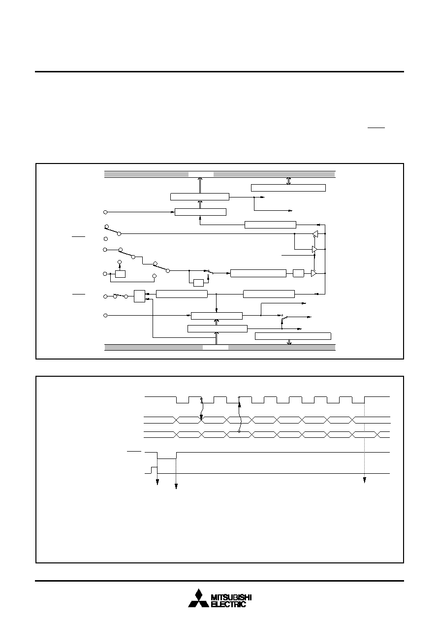
Serial I/O2
Serial I/O2 can be used as either clock synchronous or asynchro-
nous (UART) serial I/O. A dedicated timer (baud rate generator) is
also provided for baud rate generation during serial I/O2 operation.
(1) Clock synchronous serial I/O mode
The clock synchronous serial I/O mode can be selected by setting
the serial I/O2 mode selection bit (b6) of the serial I/O2 control reg-
Fig. 38 Operation of clock synchronous serial I/O2 function
Fig. 37 Block diagram of clock synchronous serial I/O2
ister (address 001D16) to “1”. For clock synchronous serial I/O, the
transmitter and the receiver must use the same clock for serial I/O2
operation. If an internal clock is used, transmit/receive is started by
a write signal to the serial I/O2 transmit/receive buffer register (TB/
RB) (address 001F16).
When P57 (SCLK22) is selected as a clock I/O pin, SRDY2 output
function is invalid, and P56 (SCLK21) is used as an I/O port.
1/4
F/F
P56/SCLK21
P54/RXD
P55/TXD
P57/SRDY2/SCLK22
“0”
“1”
“0”
“1”
XIN
1/2
XCIN
“1”
“0”
P57/SRDY2/SCLK22
Serial I/O2 status register
Serial I/O2 control register
Receive buffer register
Address 001F16
Receive shift register
Receive buffer full flag (RBF)
Receive interrupt request (RI)
Clock control circuit
Shift clock
Serial I/O2 synchronous clock selection bit
Baud rate generator
Division ratio 1/(n+1)
Address 001616
BRG count source selection bit
Clock control circuit
Falling edge detector
Transmit buffer register
Data bus
Address 001F16
Shift clock
Transmit shift register shift
completion flag (TSC)
Transmit buffer empty flag (TBE)
Transmit interrupt request (TI)
Transmit interrupt source selection bit
Address 001E16
Data bus
Address 001D16
Transmit shift register
Serial I/O2 clock I/O pin selection bit
Internal system clock selection bit
BRG clock
switch bit
Serial I/O2
clock I/O pin
selection bit
D7
D0
D1
D2
D3
D4
D5
D6
D0
D1
D2
D3
D4
D5
D6
RBF = 1
TSC = 1
TBE = 0
TBE = 1
TSC = 0
Transmit/Receive shift clock
(1/2—1/2048 of internal
clock or external clock)
Serial I/O2 output TxD
Serial I/O2 input RxD
Write-in signal to serial I/O2 transmit/receive
buffer register (address 001F16)
Overrun error (OE)
detection
Notes 1 : The transmit interrupt (TI) can be selected to occur either when the transmit buffer has emptied (TBE=1) or after the
transmit shift operation has ended (TSC=1), by setting transmit interrupt source selection bit (TIC) of the serial I/O2
control register.
2 : If data is written to the transmit buffer register when TSC=0, the transmit clock is generated continuously and serial
data is output continuously from the TxD pin.
3 : The receive interrupt (RI) is set when the receive buffer full flag (RBF) becomes “1”.
Receive enable signal SRDY2
相關PDF資料 |
PDF描述 |
|---|---|
| M39012/01-0017 | CABLE TERMINATED, MALE, N CONNECTOR, CRIMP, PLUG |
| M39012/01-0501 | CABLE TERMINATED, MALE, N CONNECTOR, CRIMP, PLUG |
| M39012/20-0006 | CABLE TERMINATED, MALE, BNC CONNECTOR, CRIMP/SOLDER, PLUG |
| M39012/26-0010 | CABLE TERMINATED, MALE, TNC CONNECTOR, CRIMP, PLUG |
| M39012/26-0012 | CABLE TERMINATED, MALE, TNC CONNECTOR, CRIMP, PLUG |
相關代理商/技術參數(shù) |
參數(shù)描述 |
|---|---|
| M38B48E2H-XXXXFP | 制造商:MITSUBISHI 制造商全稱:Mitsubishi Electric Semiconductor 功能描述:SINGLE-CHIP 8-BIT CMOS MICROCOMPUTER |
| M38B48E3H-XXXXFP | 制造商:MITSUBISHI 制造商全稱:Mitsubishi Electric Semiconductor 功能描述:SINGLE-CHIP 8-BIT CMOS MICROCOMPUTER |
| M38B48E4H-XXXXFP | 制造商:MITSUBISHI 制造商全稱:Mitsubishi Electric Semiconductor 功能描述:SINGLE-CHIP 8-BIT CMOS MICROCOMPUTER |
| M38B48E5H-XXXXFP | 制造商:MITSUBISHI 制造商全稱:Mitsubishi Electric Semiconductor 功能描述:SINGLE-CHIP 8-BIT CMOS MICROCOMPUTER |
| M38B48E6H-XXXXFP | 制造商:MITSUBISHI 制造商全稱:Mitsubishi Electric Semiconductor 功能描述:SINGLE-CHIP 8-BIT CMOS MICROCOMPUTER |
發(fā)布緊急采購,3分鐘左右您將得到回復。