- 您現(xiàn)在的位置:買(mǎi)賣(mài)IC網(wǎng) > PDF目錄359726 > M38859M6-XXXHP (Renesas Technology Corp.) SINGLE-CHIP 8-BIT CMOS MICROCOMPUTER PDF資料下載
參數(shù)資料
| 型號(hào): | M38859M6-XXXHP |
| 廠商: | Renesas Technology Corp. |
| 英文描述: | SINGLE-CHIP 8-BIT CMOS MICROCOMPUTER |
| 中文描述: | 單芯片8位CMOS微機(jī) |
| 文件頁(yè)數(shù): | 37/103頁(yè) |
| 文件大小: | 1580K |
| 代理商: | M38859M6-XXXHP |
第1頁(yè)第2頁(yè)第3頁(yè)第4頁(yè)第5頁(yè)第6頁(yè)第7頁(yè)第8頁(yè)第9頁(yè)第10頁(yè)第11頁(yè)第12頁(yè)第13頁(yè)第14頁(yè)第15頁(yè)第16頁(yè)第17頁(yè)第18頁(yè)第19頁(yè)第20頁(yè)第21頁(yè)第22頁(yè)第23頁(yè)第24頁(yè)第25頁(yè)第26頁(yè)第27頁(yè)第28頁(yè)第29頁(yè)第30頁(yè)第31頁(yè)第32頁(yè)第33頁(yè)第34頁(yè)第35頁(yè)第36頁(yè)當(dāng)前第37頁(yè)第38頁(yè)第39頁(yè)第40頁(yè)第41頁(yè)第42頁(yè)第43頁(yè)第44頁(yè)第45頁(yè)第46頁(yè)第47頁(yè)第48頁(yè)第49頁(yè)第50頁(yè)第51頁(yè)第52頁(yè)第53頁(yè)第54頁(yè)第55頁(yè)第56頁(yè)第57頁(yè)第58頁(yè)第59頁(yè)第60頁(yè)第61頁(yè)第62頁(yè)第63頁(yè)第64頁(yè)第65頁(yè)第66頁(yè)第67頁(yè)第68頁(yè)第69頁(yè)第70頁(yè)第71頁(yè)第72頁(yè)第73頁(yè)第74頁(yè)第75頁(yè)第76頁(yè)第77頁(yè)第78頁(yè)第79頁(yè)第80頁(yè)第81頁(yè)第82頁(yè)第83頁(yè)第84頁(yè)第85頁(yè)第86頁(yè)第87頁(yè)第88頁(yè)第89頁(yè)第90頁(yè)第91頁(yè)第92頁(yè)第93頁(yè)第94頁(yè)第95頁(yè)第96頁(yè)第97頁(yè)第98頁(yè)第99頁(yè)第100頁(yè)第101頁(yè)第102頁(yè)第103頁(yè)
36
3885 Group
SINGLE-CHIP 8-BIT CMOS MICROCOMPUTER
MITSUBISHI MICROCOMPUTERS
[I
2
C Data Shift Register (S0)] 0012
16
The I
2
C data shift register (S0) is an 8-bit shift register to store re-
ceive data and write transmit data.
When transmit data is written into this register, it is transferred to
the outside from bit 7 in synchronization with the S
CL
clock, and
each time one-bit data is output, the data of this register are
shifted by one bit to the left. When data is received, it is input to
this register from bit 0 in synchronization with the S
CL
clock, and
each time one-bit data is input, the data of this register are shifted
by one bit to the left. The minimum 2 cycles of
φ
are required from
the rising of the S
CL
clock until input to this register.
The I
2
C data shift register is in a write enable status only when the
I
2
C-BUS interface enable bit (ES0 bit : bit 3 S1D) of the I
2
C con-
trol register is
“
1
”
. The bit counter is reset by a write instruction to
the I
2
C data shift register. When both the ES0 bit and the MST bit
of the I
2
C status register (S1) are
“
1
”
, the S
CL
is output by a write
instruction to the I
2
C data shift register. Reading data from the I
2
C
data shift register is always enabled regardless of the ES0 bit
value.
[I
2
C Address Register (S0D)] 0013
16
The I
2
C address register (S0D) consists of a 7-bit slave address and
a read/write bit. In the addressing mode, the slave address written in
this register is compared with the address data to be received imme-
diately after the START condition is detected.
Bit 0: Read/write bit (RWB)
This is not used in the 7-bit addressing mode. In the 10-bit ad-
dressing mode, the first address data to be received is compared
with the contents (SAD6 to SAD0 + RWB) of the I
2
C address reg-
ister.
The RWB bit is cleared to
“
0
”
automatically when the stop condi-
tion is detected.
Bits 1 to 7: Slave address (SAD0–SAD6)
These bits store slave addresses. Regardless of the 7-bit address-
ing mode and the 10-bit addressing mode, the address data
transmitted from the master is compared these bits.
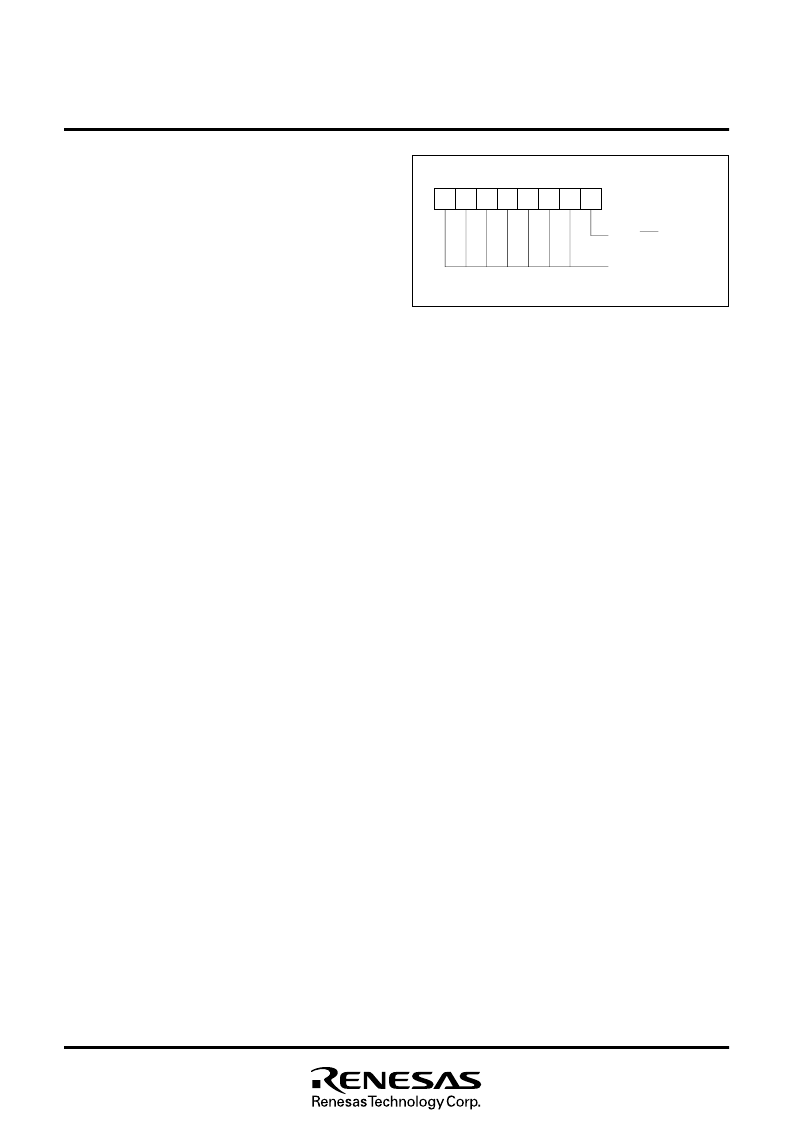
Fig. 32 Structure of I
2
C address register
SAD6 SAD5 SAD4 SAD3 SAD2 SAD1 SAD0 RWB
Slave address
I
2
C address register
(S0D: address 0013
16
)
Read/write bit
b7
b0
相關(guān)PDF資料 |
PDF描述 |
|---|---|
| M38859M7-XXXHP | SINGLE-CHIP 8-BIT CMOS MICROCOMPUTER |
| M38859M8-XXXHP | SINGLE-CHIP 8-BIT CMOS MICROCOMPUTER |
| M38859M9-XXXHP | SINGLE-CHIP 8-BIT CMOS MICROCOMPUTER |
| M38859MA-XXXHP | SINGLE-CHIP 8-BIT CMOS MICROCOMPUTER |
| M38859MB-XXXHP | SINGLE-CHIP 8-BIT CMOS MICROCOMPUTER |
相關(guān)代理商/技術(shù)參數(shù) |
參數(shù)描述 |
|---|---|
| M38859M7-XXXHP | 制造商:RENESAS 制造商全稱(chēng):Renesas Technology Corp 功能描述:SINGLE-CHIP 8-BIT CMOS MICROCOMPUTER |
| M38859M8-XXXHP | 制造商:RENESAS 制造商全稱(chēng):Renesas Technology Corp 功能描述:SINGLE-CHIP 8-BIT CMOS MICROCOMPUTER |
| M38859M9-XXXHP | 制造商:RENESAS 制造商全稱(chēng):Renesas Technology Corp 功能描述:SINGLE-CHIP 8-BIT CMOS MICROCOMPUTER |
| M38859MA-XXXHP | 制造商:RENESAS 制造商全稱(chēng):Renesas Technology Corp 功能描述:SINGLE-CHIP 8-BIT CMOS MICROCOMPUTER |
| M38859MB-XXXHP | 制造商:RENESAS 制造商全稱(chēng):Renesas Technology Corp 功能描述:SINGLE-CHIP 8-BIT CMOS MICROCOMPUTER |
發(fā)布緊急采購(gòu),3分鐘左右您將得到回復(fù)。