- 您現(xiàn)在的位置:買賣IC網(wǎng) > PDF目錄45043 > M38198ECFS 8-BIT, UVPROM, 4.2 MHz, MICROCONTROLLER, CQCC100 PDF資料下載
參數(shù)資料
| 型號: | M38198ECFS |
| 元件分類: | 微控制器/微處理器 |
| 英文描述: | 8-BIT, UVPROM, 4.2 MHz, MICROCONTROLLER, CQCC100 |
| 封裝: | CERAMIC, LCC-100 |
| 文件頁數(shù): | 106/218頁 |
| 文件大?。?/td> | 2137K |
| 代理商: | M38198ECFS |
第1頁第2頁第3頁第4頁第5頁第6頁第7頁第8頁第9頁第10頁第11頁第12頁第13頁第14頁第15頁第16頁第17頁第18頁第19頁第20頁第21頁第22頁第23頁第24頁第25頁第26頁第27頁第28頁第29頁第30頁第31頁第32頁第33頁第34頁第35頁第36頁第37頁第38頁第39頁第40頁第41頁第42頁第43頁第44頁第45頁第46頁第47頁第48頁第49頁第50頁第51頁第52頁第53頁第54頁第55頁第56頁第57頁第58頁第59頁第60頁第61頁第62頁第63頁第64頁第65頁第66頁第67頁第68頁第69頁第70頁第71頁第72頁第73頁第74頁第75頁第76頁第77頁第78頁第79頁第80頁第81頁第82頁第83頁第84頁第85頁第86頁第87頁第88頁第89頁第90頁第91頁第92頁第93頁第94頁第95頁第96頁第97頁第98頁第99頁第100頁第101頁第102頁第103頁第104頁第105頁當前第106頁第107頁第108頁第109頁第110頁第111頁第112頁第113頁第114頁第115頁第116頁第117頁第118頁第119頁第120頁第121頁第122頁第123頁第124頁第125頁第126頁第127頁第128頁第129頁第130頁第131頁第132頁第133頁第134頁第135頁第136頁第137頁第138頁第139頁第140頁第141頁第142頁第143頁第144頁第145頁第146頁第147頁第148頁第149頁第150頁第151頁第152頁第153頁第154頁第155頁第156頁第157頁第158頁第159頁第160頁第161頁第162頁第163頁第164頁第165頁第166頁第167頁第168頁第169頁第170頁第171頁第172頁第173頁第174頁第175頁第176頁第177頁第178頁第179頁第180頁第181頁第182頁第183頁第184頁第185頁第186頁第187頁第188頁第189頁第190頁第191頁第192頁第193頁第194頁第195頁第196頁第197頁第198頁第199頁第200頁第201頁第202頁第203頁第204頁第205頁第206頁第207頁第208頁第209頁第210頁第211頁第212頁第213頁第214頁第215頁第216頁第217頁第218頁
180
3. APPENDIX
MITSUBISHI MICROCOMPUTER
3819 Group
3.3 Control registers
3819 Group USER’S MANUAL
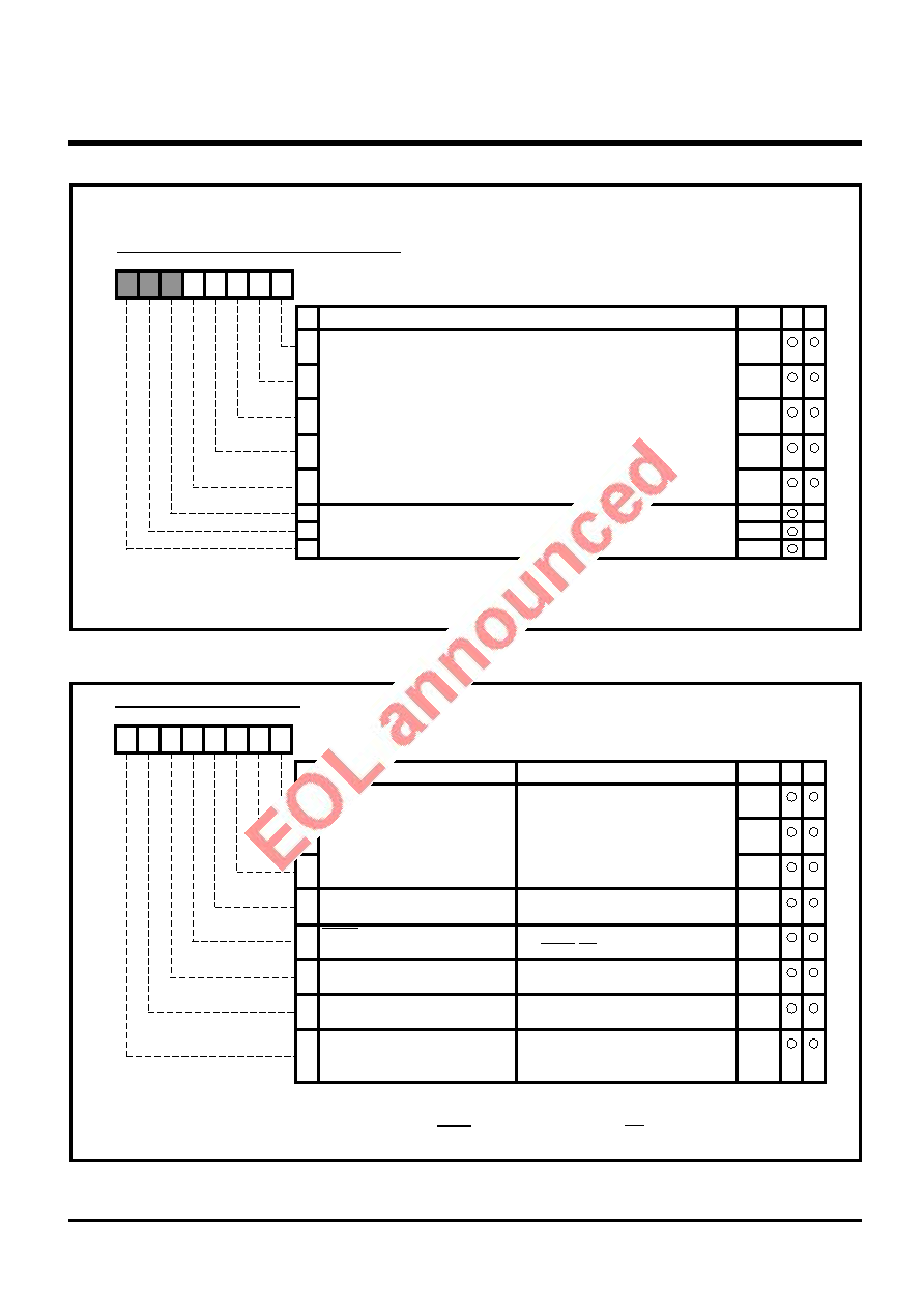
Fig. 3.3.3 Structure of Serial I/O automatic transfer data pointer
Fig. 3.3.4 Structure of Serial I/O 1 control register
When an external clock is selected in the serial I/O 1 automatic transfer
mode, the S RDY1 signal pin is used as the CS signal input pin.
Serial I/O automatic transfer data pointer
b7 b6 b5 b4 b3 b2 b1 b0
B
Function
At reset
RW
0
1
2
3
4
6
7
0
Serial I/O automatic transfer data pointer (SIODP) [Address:1816]
0
Nothing is allocated for these bits. These are write disabled bits.
When these bits are read out, the values are "0."
Indicate an address of Serial I/O automatic transfer RAM.
?
0
5
!
Serial I/O 1 control register
b7 b6 b5 b4 b3 b2 b1 b0
B
Function
At reset
RW
0
1
2
3
4
5
6
7
0
Serial I/O 1 control register (SIO1CON) [Address:1916]
Name
Internal synchronous clock
selection bits
Synchronous clock selection
bit
000 : f(XIN)/8 or f(XCIN)/8
001 : f(XIN)/16 or f(XCIN)/16
010 : f(XIN)/32 or f(XCIN)/32
011 : f(XIN)/64 or f(XCIN)/64
110 : f(XIN)/128 or f(XCIN)/128
111 : f(XIN)/256 or f(XCIN)/256
0 : External clock
1 : Internal clock
P65/SOUT1 P-channel output
disable bit
b2 b1b0
Serial I/O 1 port selection bit
(P65,P66,P67 )
T
Transfer direction selection
bit
0 : LSB first
1 : MSB first
SRDY1 output selection bit
(P67)
0 : I/O port
1 : SRDY1/CS signal pin
( Note)
0 : I/O port
1 : SOUT1, SCLK11, SCLK12 signal pins
T
Valid only in the Serial I/O automatic transfer mode
0 : CMOS output (in output mode)
1 : N-channel open-drain output
(in output mode)
Note :
相關PDF資料 |
PDF描述 |
|---|---|
| M38199MF-XXXFP | 8-BIT, MROM, 4.2 MHz, MICROCONTROLLER, PQFP100 |
| M38199EFFP | 8-BIT, OTPROM, MICROCONTROLLER, PQFP100 |
| M38198EC-XXXFP | 8-BIT, OTPROM, MICROCONTROLLER, PQFP100 |
| M38199MF-XXXKP | 8-BIT, MROM, MICROCONTROLLER, PQFP100 |
| M38198MC-XXXKP | 8-BIT, MROM, MICROCONTROLLER, PQFP100 |
相關代理商/技術參數(shù) |
參數(shù)描述 |
|---|---|
| M38198MCA809 | 制造商:Panasonic Industrial Company 功能描述:IC |
| M38198MCA824 | 制造商:Panasonic Industrial Company 功能描述:IC |
| M38198MCA827 | 制造商:Panasonic Industrial Company 功能描述:IC |
| M38199MF072F | 制造商:Panasonic Industrial Company 功能描述:IC |
| M38199MF210F | 制造商:Panasonic Industrial Company 功能描述:IC |
發(fā)布緊急采購,3分鐘左右您將得到回復。